
A cspbbr induced by tensile strain 3 ferroelectric single crystal thin film method
A single crystal thin film, tensile strain technology, applied in the direction of single crystal growth, single crystal growth, chemical instruments and methods, etc., can solve the problems of cumbersome preparation process, complicated way of applying stress, and failure to meet the use requirements, etc., to achieve operational Simple, low-cost effect
Patent Information
- Authority / Receiving Office
- CN · China
- Patent Type
- Patents(China)
- Current Assignee / Owner
- Publication Date
- 2022-04-08
Smart Images
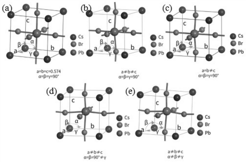
Figure 1 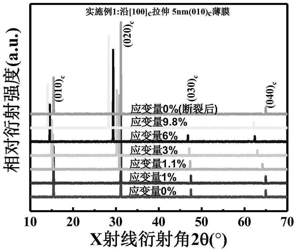
Figure 2 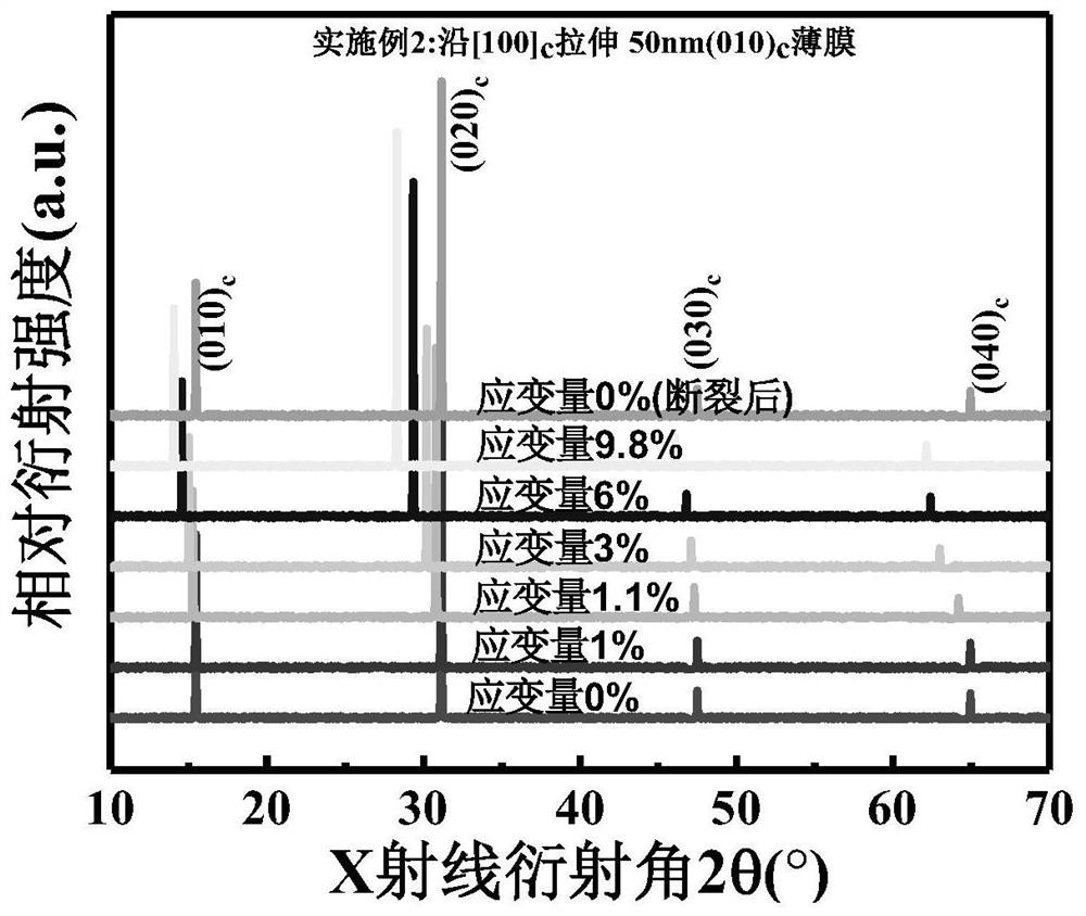
Figure 3
Abstract
Description
technical field
[0001] The invention relates to the field of ferroelectric perovskite technology, in particular to a CsPbBr ferroelectric perovskite induced by tensile strain 3 method for ferroelectric single crystal thin films. Background technique
[0002] In recent years, all-inorganic halide perovskites have become a new generation of highly competitive optoelectronic functional materials due to their excellent stability and optoelectronic properties, and have been widely used in solar cells, photodetection, light-emitting diodes, LEDs and other fields. Among them, the all-inorganic perovskite CsPbBr 3 Due to its excellent high temperature and high humidity resistance, low production cost, high light absorption coefficient, high carrier mobility and high open circuit voltage, it has attracted great attention from researchers.
[0003] At present, the vast majority of semiconductor and microelectronic devices can be prepared from the material Si, including N-type semico...
Examples
Embodiment 1
[0042] A CsPbBr induced by tensile strain 3 The method for ferroelectric single crystal thin film, the operation link of described method is as follows:
[0043] Link 1, CsPbBr 3 Single crystal preparation
[0044] (1) CsBr and PbBr with a molar ratio of 1:1 2 The mixture of was dissolved in dimethylformamide (DMF) to form a supersaturated solution with a concentration of 1.5 mol / L, and was fully stirred at 70°C.
[0045] (2) The supersaturated solution was heated to 150°C, and the suspended insoluble matter was filtered out, and the solution was gradually cooled to 70°C and kept for 10 hours to grow seed crystals.
[0046] (3) Prepare a new supersaturated solution according to step (1), put the seed crystal obtained in step (2) into it to obtain a larger seed crystal, repeat three times and then put the seed crystal into anti-solvent toluene to keep room temperature High quality CsPbBr of desired size can be obtained in 7 days 3 For a single crystal, the side length of t...
Embodiment 2
[0066] This embodiment prepares CsPbBr in the same manner as in Example 1 3 Single crystal thin film is also stretched and tested in the same manner as in Example 1, the difference being that:
[0067] In link 2 step (5), preferably, after the second thinning treatment, CsPbBr 3 The thickness of the single crystal thin film is 50nm.
[0068] In link 4 step (1), when the strain amount is 1.1%, its saturated ferroelectric polarization is 0.10μC / cm 2 ; When the strain amount is 3%, its saturated ferroelectric polarization is 0.18μC / cm 2 ; When the strain is 6%, its saturated ferroelectric polarization is 0.27μC / cm 2 ; When the strain amount is 9.8%, its saturated ferroelectric polarization is 0.42μC / cm 2 . Test obtains this embodiment CsPbBr 3 The XRD patterns of the single crystal film before and after stretching and during stretching are as follows: image 3 As shown, the data of the lattice constant and its crystal system, point group, saturated ferroelectric polarizati...
Embodiment 3
[0070] A CsPbBr induced by tensile strain 3 The method for ferroelectric single crystal thin film, the operation link of described method is as follows:
[0071] Link 1, CsPbBr 3 Single crystal preparation
[0072] (1) CsBr and PbBr with a molar ratio of 1:1 2 The mixture of was dissolved in dimethylformamide (DMF) to form a supersaturated solution with a concentration of 1.5 mol / L, and was fully stirred at 70°C.
[0073] (2) The supersaturated solution was heated to 150°C, and the suspended insoluble matter was filtered out, and the solution was gradually cooled to 70°C and kept for 10 hours to grow seed crystals.
[0074] (3) Prepare a new supersaturated solution according to step (1), put the seed crystal obtained in step (2) into it to obtain a larger seed crystal, repeat three times and then put the seed crystal into anti-solvent toluene to keep room temperature High quality CsPbBr of desired size can be obtained in 7 days 3 For a single crystal, the side length of t...