Supercharge Your Innovation With Domain-Expert AI Agents!

Photoelectric switch chip production device and method

A photoelectric switch and chip technology, which is applied in the manufacture of circuits, electrical components, and final products, can solve the problems of reduced chip production and processing efficiency, reduced silicon wafer cleaning effect, and secondary pollution on the silicon wafer surface, so as to improve transmission and absorption Efficiency, simplified packaging process, simplified processing effect

Active Publication Date: 2021-11-12
无锡光磊电子科技有限公司
View PDF3 Cites 0 Cited by
  • Summary
  • Abstract
  • Description
  • Claims
  • Application Information

AI Technical Summary

Problems solved by technology

[0005] In order to make up for the deficiencies of the existing technology, solve the problem of brushing and cleaning the surface of the silicon wafer. When the brush head contacts the surface of the silicon wafer again, the impurities in the brush head are driven by the brush head to contact the surface of the silicon wafer again, so that the surface of the silicon wafer contacts again. Impurities in the brush head lead to secondary pollution on the surface of the silicon wafer, thereby reducing the cleaning effect of the silicon wafer, and further reducing the cleaning efficiency of the silicon wafer, resulting in a problem that the production and processing efficiency of the chip is reduced. The invention proposes a photoelectric switch chip. Preparation equipment and method

Method used


Image

  • Photoelectric switch chip production device and method
  • Photoelectric switch chip production device and method
  • Photoelectric switch chip production device and method

Examples


Embodiment approach

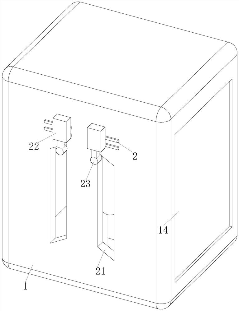
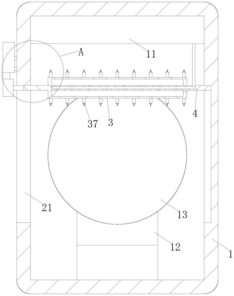
[0036] As an embodiment of the present invention, the second hole 32 is a tapered hole, and the diameter of the second hole 32 close to the fixed shaft 4 is larger than the diameter of the second hole 32 away from the fixed shaft 4 .

[0037] When in use, the rotating tube 3 drives the No. 3 plate 36 to move, and the end of the No. 3 plate 36 close to the fixed shaft 4 is attached to the surface of the rotating tube 3. The No. 3 plate 36 moves until it touches the No. 2 plate 34 and pushes the No. 2 plate 34 to move. The third plate 36 pushes the second plate 34 to move with the fixed shaft 4 as the center of circle, and the third plate 36 squeezes the cleaning liquid between the second plate 34 and the third plate 36 in the rotating tube 3, and the cleaning liquid is affected by gravity and the second plate 36. Under the extrusion force produced between the No. plate 34 and the No. three plate 36, the cleaning liquid flows out through the No. 2 hole 32. Since the No. 2 hole 32...


PUM


Abstract

The invention belongs to the technical field of photoelectric switch chip processing, and particularly relates to a photoelectric switch chip production device and method.The photoelectric switch chip production device comprises a shell, a hydraulic unit, a motor and a clamping unit; a spraying unit is fixedly connected to the top of the interior of the shell, a clamping unit is fixedly connected to the center of the bottom of the interior of the shell, and a silicon wafer is installed on the clamping unit; placing doors are formed in the two sides of the shell; and a second hole is formed, a rotating pipe drives a third plate to move, the third plate moves to make contact with the second plate and then pushes the second plate to move, the second plate extrudes a cleaning liquid located between the second plate and the first plate in the rotating pipe, and the cleaning liquid flows to a brush from the second hole. Impurities attached to a cleaning liquid film layer on the surface of a silicon wafer brushed by the brush are washed away, and the cleaning degree of the brush is increased so that the cleaning degree of the surface of the silicon wafer is increased, and the processing efficiency of the silicon wafer is improved.

Description

technical field [0001] The invention belongs to the technical field of photoelectric switch chip processing, in particular to a preparation device and method for a photoelectric switch chip. Background technique [0002] Photoelectric switch is the abbreviation of photoelectric proximity switch. It uses the blocking or reflection of the light beam by the detected object, and the synchronous circuit is connected to the circuit to detect the presence or absence of the object. The photoelectric switch chip is an important part of the photoelectric switch. The integrated circuit combines multiple components on one chip, which improves the performance of the chip and reduces the cost. With the introduction of silicon materials, the chip process has gradually evolved to deposit devices on the upper layer of the silicon chip and the substrate of the circuit layer; among them, there are five main steps in the production of photoelectric switch chips made of silicon: silicon chip pre...

Claims


Application Information

Patent Timeline
IPC IPC(8): H01L21/67H01L31/18H01L21/02H01L31/12
CPCH01L21/67046H01L21/67051H01L31/1804H01L21/02057H01L21/02082H01L31/125Y02P70/50
Inventor 姚磊唐红祥何飞
Owner 无锡光磊电子科技有限公司
Features
  • R&D
  • Intellectual Property
  • Life Sciences
  • Materials
  • Tech Scout
  • Unparalleled Data Quality
  • Higher Quality Content
  • 60% Fewer Hallucinations
Learn More