LED chip, preparation method thereof and display device

A technology of LED chips and semiconductors, which is applied in the direction of electrical components, electrical solid devices, circuits, etc., can solve the problems of low light extraction efficiency of LEDs, and achieve the goal of improving light extraction efficiency, reducing light reflection, improving light extraction efficiency and luminous efficiency Effect

Pending Publication Date: 2021-11-12
CHONGQING KONKA PHOTOELECTRIC TECH RES INST CO LTD
View PDF0 Cites 0 Cited by
  • Summary
  • Abstract
  • Description
  • Claims
  • Application Information

AI Technical Summary

Problems solved by technology

[0004] The purpose of the embodiments of the present invention is to provide an LED chip, aiming to solve the problem of low light extraction efficiency of existing LEDs

Method used


Image

  • LED chip, preparation method thereof and display device
  • LED chip, preparation method thereof and display device
  • LED chip, preparation method thereof and display device

Examples


Embodiment Construction

[0027] In order to make the object, technical solution and advantages of the present invention clearer, the present invention will be further described in detail below in conjunction with the accompanying drawings and embodiments. It should be understood that the specific embodiments described here are only used to explain the present invention, not to limit the present invention.

[0028] In addition, in the description of the present application, the terms used should be interpreted in a broad sense, and those skilled in the art can understand the specific meanings of the terms according to actual specific situations. For example, the terms "setting" and "with" used in this application can be defined as contact setting or non-contact setting, etc.; The direction defined by common knowledge shall prevail.

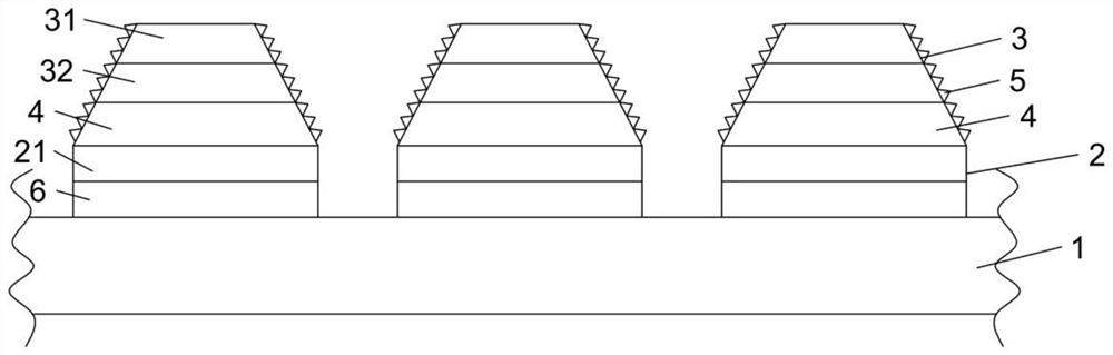
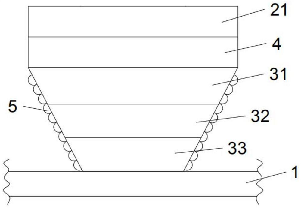
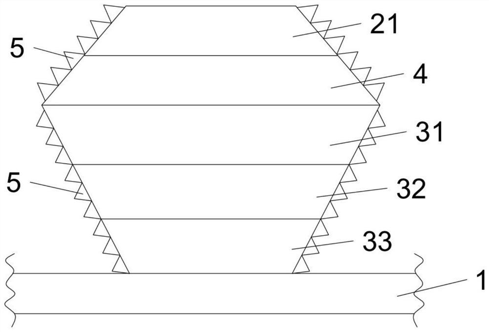
[0029] as attached figure 1 As shown, the embodiment of the present invention provides an LED chip, which includes a substrate 1 and at least one set of epitaxial layers...


PUM

PropertyMeasurementUnit
angleaaaaaaaaaa

Abstract

The invention is applicable to the technical field of LEDs, and provides an LED chip, a preparation method thereof and a display device. The LED chip comprises a substrate and at least one set of epitaxial layers arranged on the substrate, each epitaxial layer comprises a first semiconductor layer and a second semiconductor layer, and a quantum well layer is arranged between the first semiconductor layer and the second semiconductor layer; at least part of the side surface of at least one of the first semiconductor layer, the second semiconductor layer and the quantum well layer is a rough surface, and a first included angle is formed between the rough surface and the longitudinal axis of the substrate. The LED chip provided by the embodiment of the invention is provided with the inclined and rough side surface which can cause light movement disorder, reduce light reflection in the LED chip and enable more light to meet an escape angle, so that the light extraction efficiency of the LED chip is improved.

Description

technical field [0001] The invention belongs to the technical field of LEDs, and in particular relates to an LED chip, a preparation method thereof, and a display device. Background technique [0002] Generally speaking, the external quantum efficiency of a light emitting diode (Light Emitting Diode, LED) is equal to the product of the internal quantum efficiency and the light extraction efficiency. Therefore, in order to improve the external quantum efficiency of the LED, it is necessary to increase the light extraction efficiency of the LED. [0003] Due to the difference in refractive index between gallium nitride and air in the LED chip, the critical angle is very small, which leads to total reflection of light inside the LED chip, which will lead to low light extraction efficiency of the LED and affect the external quantum efficiency of the LED. . Contents of the invention [0004] The purpose of the embodiments of the present invention is to provide an LED chip, aim...

Claims


Application Information

Patent Timeline
Patent Type & Authority Applications(China)
IPC IPC(8): H01L33/06H01L33/20H01L33/22H01L33/00H01L27/15
CPCH01L33/06H01L33/20H01L33/22H01L33/0075H01L27/156
Inventor 张雪林子平李刘中安金鑫肖守均
Owner CHONGQING KONKA PHOTOELECTRIC TECH RES INST CO LTD
Why Eureka
Try Eureka