Check patentability & draft patents in minutes with Patsnap Eureka AI!

Pixel structure, array substrate and display panel

A pixel structure and array substrate technology, applied in nonlinear optics, instruments, optics, etc., can solve the problems of 8-domain display panel structure and manufacturing complexity, and achieve reduced structural complexity and manufacturing costs, low structural complexity and manufacturing Cost, effect of reducing manufacturing steps

Pending Publication Date: 2021-11-19
BEIHAI HKC OPTOELECTRONICS TECH CO LTD +1
View PDF0 Cites 2 Cited by
  • Summary
  • Abstract
  • Description
  • Claims
  • Application Information

AI Technical Summary

Problems solved by technology

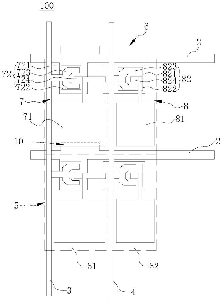
[0004] The purpose of the embodiment of the present application is to provide a pixel structure, aiming to solve the technical problems of the existing 8-domain display panel with relatively complex structure and fabrication

Method used


Image

  • Pixel structure, array substrate and display panel
  • Pixel structure, array substrate and display panel
  • Pixel structure, array substrate and display panel

Examples


Embodiment Construction

[0044] In order to make the purpose, technical solution and advantages of the present application clearer, the present application will be further described in detail below in conjunction with the accompanying drawings and embodiments. It should be understood that the specific embodiments described here are only used to explain the present application, not to limit the present application.

[0045]It should be noted that when a component is referred to as being “fixed on” or “disposed on” another component, it may be directly or indirectly fixed or disposed on the other component. When an element is referred to as being "connected to" another element, it can be directly or indirectly connected to the other element. The orientation or positional relationship indicated by the terms "upper", "lower", "left", "right", etc. are based on the orientation or positional relationship shown in the drawings, and are for convenience of description only, rather than indicating or implying t...


PUM


Abstract

The invention is suitable for the technical field of display and provides a pixel structure, an array substrate and a display panel. The pixel structure comprises a scanning line, data lines and a pixel unit, wherein the pixel unit comprises a main pixel unit and an auxiliary pixel unit; a plurality of sub drive lines are further included, and the data lines are parallel to the sub drive lines and arranged at intervals, the main pixel unit comprises a main pixel electrode and a main thin film transistor, a first grid electrode of the main thin film transistor is connected with the scanning line, a first source electrode of the main thin film transistor is connected with the data lines, and a first drain electrode of the main thin film transistor is connected with the main pixel electrode; the auxiliary pixel unit comprises an auxiliary pixel electrode and an auxiliary thin film transistor, a second grid electrode of the auxiliary thin film transistor is connected with the first drain electrode, a second source electrode is connected with an auxiliary driving line, and a second drain electrode is connected with the auxiliary pixel electrode; according to the pixel structure, eight domains can be realized on the basis of two TFTs, the number and manufacturing steps of the TFTs are reduced on the basis of ensuring a large-angle viewing angle range, and structural complexity and manufacturing cost of the pixel structure are reduced.

Description

technical field [0001] The present application relates to the field of display technology, in particular to a pixel structure, an array substrate and a display panel. Background technique [0002] TFT-LCD (Thin Film Transistor-Liquid Crystal Display) has a variety of commonly used display modes, such as TN (Twisted Nematic, twisted nematic) display mode, VA (Vertically Alignment, vertical alignment) display mode, FFS (Fringe Field Switching, fringe field switching) display mode, and IPS (In-Plane Switching, in-plane switching) display mode, etc. Among them, VA mode has better dark state performance and better contrast than other display modes, but its viewing angle is relatively poor. [0003] At present, the method of dividing pixels into multiple domains (Domain) is often used to improve the viewing angle of VA display, such as 8 domain and 4 domain. The 4domain is usually formed by forming slits on the pixel electrodes and protrusions on the color filter substrate. The ...

Claims


Application Information

Patent Timeline
IPC IPC(8): G02F1/1362G02F1/1343G02F1/1368
CPCG02F1/136286G02F1/1362G02F1/134309G02F1/1368
Inventor 蒲洋刘振洪文进许哲豪袁海江
Owner BEIHAI HKC OPTOELECTRONICS TECH CO LTD
Features
  • R&D
  • Intellectual Property
  • Life Sciences
  • Materials
  • Tech Scout
  • Unparalleled Data Quality
  • Higher Quality Content
  • 60% Fewer Hallucinations
Learn More