Light-emitting diode chip and display device

A technology of light-emitting diodes and chips, which is applied in the direction of identification devices, instruments, electrical components, etc., to reduce differences, improve display effects, and reduce pixel pitch.

Active Publication Date: 2021-11-19
BOE TECH GRP CO LTD +1
View PDF6 Cites 1 Cited by
  • Summary
  • Abstract
  • Description
  • Claims
  • Application Information

AI Technical Summary

Problems solved by technology

[0004] Embodiments of the present disclosure provide a light emitting diode chip and a display device to solve or alleviate one or more technical problems in the prior art

Method used


Image

  • Light-emitting diode chip and display device
  • Light-emitting diode chip and display device
  • Light-emitting diode chip and display device

Examples


Embodiment Construction

[0068] In the following, only some exemplary embodiments are briefly described. As those skilled in the art would realize, the described embodiments may be modified in various different ways, all without departing from the spirit or scope of the present disclosure. Accordingly, the drawings and descriptions are to be regarded as illustrative in nature and not restrictive.

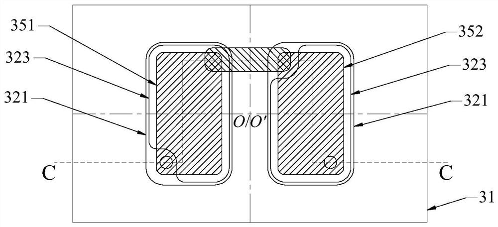
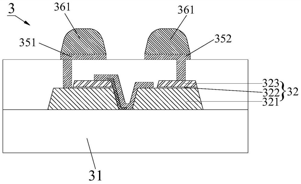
[0069] In order to reduce costs, glass-based TFT circuit substrates are the ideal carrier substrates for next-generation display products. In order to cooperate with TFT substrates and reduce overall power consumption, high-voltage LED chips can be preferred. figure 1 It is a top view structural schematic diagram of an LED chip, figure 2 for figure 1 Schematic diagram of the C-C cross-sectional structure in . Such as figure 1 and figure 2 As shown, the LED chip 3 may be a high-voltage LED chip, and the LED chip 3 may include two light emitting parts 32 .

[0070] Exemplarily, as figure 2 As shown,...


PUM

PropertyMeasurementUnit
heightaaaaaaaaaa
thicknessaaaaaaaaaa
thicknessaaaaaaaaaa

Abstract

The embodiment of the invention provides a light-emitting diode chip and a display device. The light-emitting diode chip includes a substrate, a light-emitting structure located on one side of the substrate, a first electrode and a second electrode located on the side, away from the substrate, of the light-emitting structure. The first electrode and the second electrode are connected with the light-emitting structure, and the light-emitting structure is configured to generate light under the voltage difference effect of the first electrode and the second electrode; the light-emitting center of the light-emitting diode chip has a preset offset relative to the geometric center of the substrate, and the light-emitting center of the light-emitting diode chip is the geometric center of the orthographic projection of the light-emitting area of the light-emitting structure on the substrate. According to the technical scheme, when the LED chips are arranged on the back plate, the light-emitting centers of the sub-pixels in the pixels can be more concentrated, the light-emitting areas of the pixels are more concentrated, the visual difference is reduced, and the display effect is improved; in addition, the pixel pitch can be reduced, and the resolution of the display device is improved.

Description

technical field [0001] The present disclosure relates to the field of display technology, in particular to a light emitting diode chip and a display device. Background technique [0002] Light-emitting diode (Light-Emitting Diode, LED) chips, as a key technology of display technology, have become a trend in the display industry. How to improve the performance of LED display products and enhance product competitiveness has become the direction of the joint efforts of the display industry. [0003] In the existing LED display products, the size of the LED chip is large, which is limited by the size of the LED chip, the pixel pitch is large, and the pixel segmentation is serious, so it is difficult to achieve high resolution. Contents of the invention [0004] Embodiments of the present disclosure provide a light emitting diode chip and a display device to solve or alleviate one or more technical problems in the prior art. [0005] As a first aspect of the embodiments of th...

Claims


Application Information

Patent Timeline
Patent Type & Authority Applications(China)
IPC IPC(8): H01L33/08H01L33/06H01L33/36H01L25/16G09F9/33
CPCH01L33/08H01L33/06H01L33/36H01L25/167G09F9/33
Inventor 卢元达岂林霞杨山伟赵加伟熊志军孙元浩张方振
Owner BOE TECH GRP CO LTD
Why Eureka
Try Eureka