Wafer bearing system with high etching rate uniformity and wafer bearing disc structure thereof

A wafer carrying and etching rate technology, applied in discharge tubes, electrical components, circuits, etc., can solve the problems of poor etching rate uniformity and poor temperature uniformity, achieve optimal etching rate uniformity, and improve temperature uniformity. Sexuality, the effect of increasing efficiency

Pending Publication Date: 2021-11-30
HERMES EPITEK
View PDF0 Cites 0 Cited by
  • Summary
  • Abstract
  • Description
  • Claims
  • Application Information

AI Technical Summary

Problems solved by technology

[0005] The invention is a wafer carrying system with high etch rate uniformity and its wafer carrier, which mainly solves the convenience of placing and taking out the wafer carrier on the wafer surface, and the uniform temperature between the surfaces of each wafer Poor performance, resulting in poor etch rate uniformity

Method used


Image

  • Wafer bearing system with high etching rate uniformity and wafer bearing disc structure thereof
  • Wafer bearing system with high etching rate uniformity and wafer bearing disc structure thereof
  • Wafer bearing system with high etching rate uniformity and wafer bearing disc structure thereof

Examples


Embodiment Construction

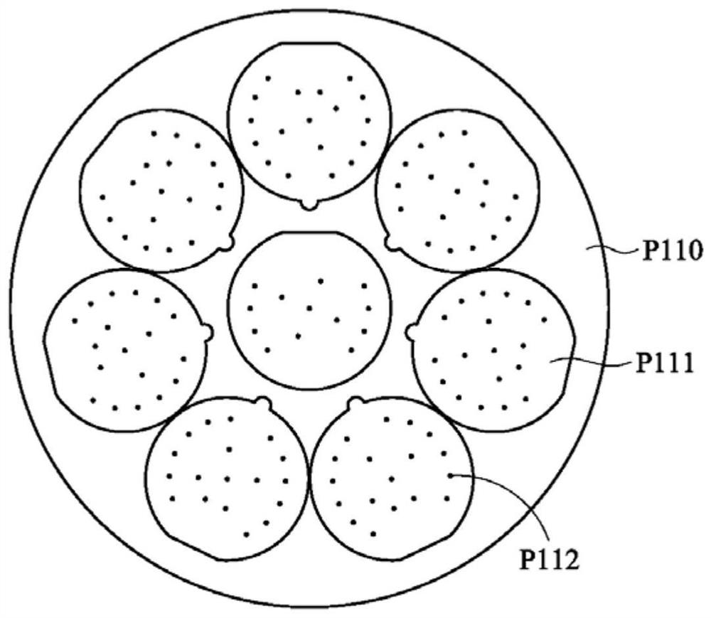
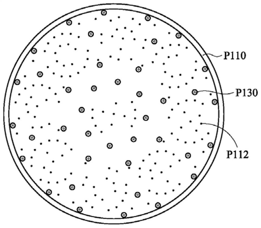
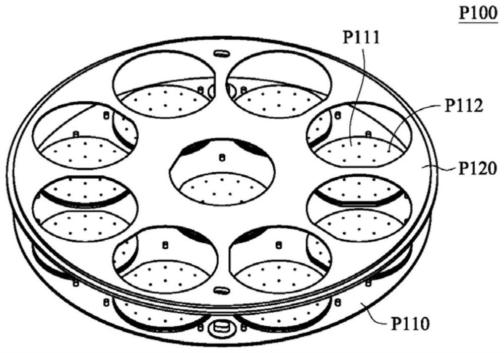
[0067] As shown in FIG. 4 , the present embodiment is a wafer carrier system 100 with high etch rate uniformity, which includes: a lower electrode base plate 110 ; a lower electrode upper cover plate 120 ; a high etch rate uniformity wafer carrier 130 ; And the outgassing seal ring 140 .

[0068] The lower electrode base plate 110 is used for connecting a radio frequency (RF), so that the positively charged particles are attracted by the negative bias and accelerated, and then almost vertically perform ion-bombardment on the wafer placed on the bearing surface 131a ) to produce an etch rate response. In order to control or cool the wafer, the lower electrode base plate 110 has cooling medium injection holes 111 , cooling medium discharge holes 112 and a plurality of air inlet holes 113 for cooling medium.

[0069] The cooling medium injection hole 111 can be used to inject a cooling medium such as water, and the cooling medium discharge hole 112 can be used to discharge the c...


PUM


Abstract

The invention relates to a wafer bearing system with high etching rate uniformity and a wafer bearing disc structure thereof. The wafer bearing system comprises a lower electrode bottom plate; a lower electrode upper cover plate which is provided with a temperature adjusting flow channel which forms a positive flow direction; a plurality of fluid channels which are communicated with the air inlet hole of the lower electrode bottom plate; a high-etching-rate uniformity wafer loading disc, wherein a temperature adjusting layer is formed by the bottom surface of a body of the high-etching-rate uniformity wafer loading disc and the lower electrode upper cover plate; a plurality of temperature adjusting blocks which are formed on the bottom surface, wherein each temperature adjusting block is formed by at least one temperature adjusting groove and forms a block temperature adjusting volume, and the size of the block temperature adjusting volume is gradually increased according to the sequence of the forward flow direction; and a gas permeation sealing ring which is arranged between the outer edge of the high etching rate uniformity wafer loading disc and the lower electrode upper cover plate. According to the embodiment of the invention, the temperature of the wafer carrying disc can be adjusted through the temperature adjusting block, so the effect of high etching rate uniformity is achieved, and in addition, the arrangement or taking-out of the wafer can be more conveniently completed.

Description

technical field [0001] The present invention relates to a wafer carrier system with high etching rate uniformity and a wafer carrier thereof, especially a wafer carrier system with high etching rate uniformity for semiconductor or optoelectronic components and a wafer with high etching rate uniformity thereof. Load disk. Background technique [0002] like 1A to 2B As shown, in the equipment of the etching machine, in order to effectively maintain the optimal temperature and uniformity of the surface of the workpiece to be processed, such as a wafer, various temperature adjustment mechanisms are designed, among which 1A to 2B It is a two-piece wafer carrier structure P100, which is a conventional wafer placement area P111 on the conventional wafer carrier P110, and a plurality of temperature-regulated air holes P112 are provided. The fluid injected by P112 controls the temperature of the wafer, but in this design, in order to prevent the wafer from being lifted or sprayed b...

Claims


Application Information

Patent Timeline
Patent Type & Authority Applications(China)
IPC IPC(8): H01J37/32
CPCH01J37/32724H01J2237/334
Inventor 吴胜华林志隆彭于容陈俊龙
Owner HERMES EPITEK
Why Eureka
Try Eureka