A semiconductor packaging device

A technology for packaging devices and semiconductors, which can be applied to devices that apply liquid to surfaces, semiconductor/solid-state device manufacturing, and coating. Avoid the effect of height reduction, increase dispensing range, and increase the rate of packaging

Active Publication Date: 2022-02-08
天霖(张家港)电子科技有限公司
View PDF6 Cites 0 Cited by
  • Summary
  • Abstract
  • Description
  • Claims
  • Application Information

AI Technical Summary

Problems solved by technology

[0006] Aiming at the deficiencies of the prior art, the present invention provides a semiconductor packaging device, which solves the problem that when the packaging gaps of semiconductors are different in size during packaging, the gaps still appear after packaging, which reduces the sealing performance of semiconductors during storage, and at the same time the sealing of semiconductors after packaging The cooling rate of the semiconductor is slow, and it is easy to cause the problem of adhesion to other parts and damage the semiconductor during storage.

Method used


Image

  • A semiconductor packaging device
  • A semiconductor packaging device
  • A semiconductor packaging device

Examples


Embodiment 1

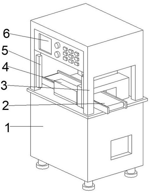
[0043] see Figure 1-6 , the present invention provides a technical solution: a semiconductor packaging device, including a device body 1, a processing frame 3 is fixedly connected to the top of the device body 1, and a feeding frame 2 is fixedly connected to the middle position of the bottom of the inner cavity of the processing frame 3. Driven by the power parts, the frame 2 transports the semiconductor to the encapsulation dispensing position for encapsulation, which effectively improves the rate of encapsulation and avoids the deviation of the dispensing position caused by the offset of placement, and the bottom of the inner cavity of the processing frame 3 is fixed The packaging device 4 is connected, the front bottom of the packaging device 4 penetrates the feeding rack 2 and extends to the outside of the feeding rack 2, the front top of the processing frame 3 is fixedly connected to the control panel 6, and the front and bottom sides of the processing frame 3 are fixedly...

Embodiment 2

[0050] see Figure 1-6, on the basis of Embodiment 1, the present invention provides a technical solution: a method for using a semiconductor packaging device, step 1: install and fix the equipment, and fix the equipment main body 1 with the processing frame 3, and feed the The frame 2 is fixedly connected to the packaging device 4, and the equipment main body 1 is connected to the energy source, and the detection light curtain 5 is fixedly connected to the processing frame 3;

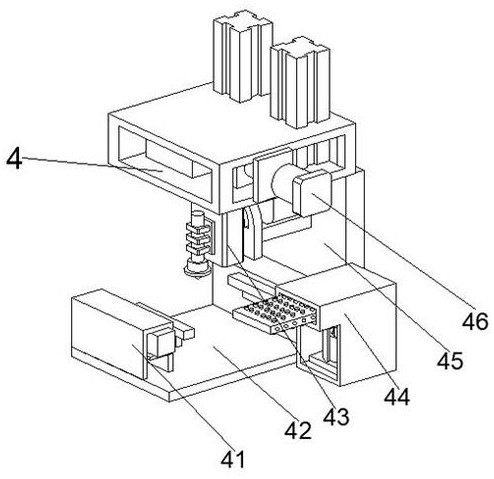
[0051] Step 2: Use the dispensing cavity produced by the glue dispenser 43 and the packaging fixture 41 to apply glue at fixed points, and when the semiconductor is fixed, it is in the center position, and the guide device 44 is fixedly connected to the carrier plate 42, and the carrier plate 42 is fixed. It is fixedly connected with the packaging fixture 41, so that the semiconductor is fixed to the dispenser 43;

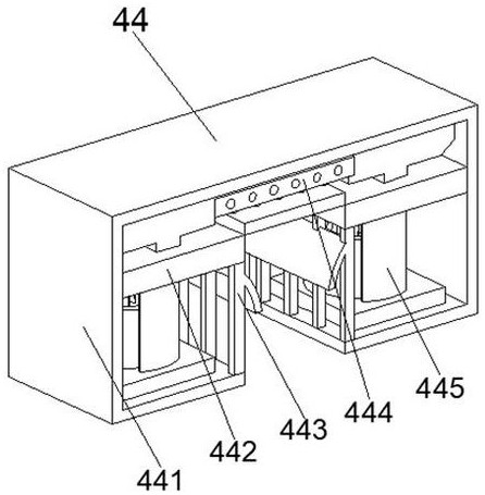
[0052] Step 3: Use the cold air blown by the cooling plate 444 to contact the dispensi...


PUM


Abstract

The invention discloses a semiconductor packaging device, which comprises a device main body. A processing frame is fixedly connected to the top of the device main body. A feeding frame is fixedly connected to the middle of the inner cavity bottom of the processing frame. The front bottom of the packaging device penetrates the feeding frame and extends to the feeding frame. Outside the frame, a control panel is fixedly connected to the front top of the processing frame, and detection light curtains are fixedly connected to both sides of the front bottom of the processing frame. The invention relates to the technical field of semiconductor packaging. The semiconductor encapsulation device effectively improves the rate of encapsulation. The dispensing machine reciprocates clockwise or counterclockwise on the adjustment device, thereby deflecting the dispensing position and effectively increasing the dispensing of the semiconductor fixed position. Range, the transmission part can drive the adjustment device to adjust the glue dispenser, which is convenient to ensure that the glue dispenser and the semiconductor maintain a suitable height of dispensing, and is conducive to avoiding the height reduction between the glue dispenser and the semiconductor.

Description

technical field [0001] The invention relates to the technical field of semiconductor packaging, in particular to a semiconductor packaging device. Background technique [0002] Semiconductor packaging refers to the process of processing the tested wafers according to the product model and functional requirements to obtain independent chips. The packaging process is: the wafer from the wafer front-end process is cut into small chips (Die) after the dicing process, and then the cut chip is glued to the island of the corresponding substrate (lead frame) frame Then use ultra-fine metal (gold-tin-copper-aluminum) wires or conductive resin to connect the bonding pads (Bond Pad) of the chip to the corresponding pins (Lead) of the substrate to form the required circuit. [0003] According to a semiconductor packaging device disclosed in Chinese Patent No. CN112289717A, the rotation of the first transmission motor drives the first helical gear connected to it to rotate, the rotation...

Claims


Application Information

Patent Timeline
Patent Type & Authority Patents(China)
IPC IPC(8): H01L21/67B05C5/02B05C11/10B05C9/14B05C13/02B05D3/00
CPCH01L21/67121H01L21/6715B05C5/0212B05C11/1018B05C11/10B05C9/14B05C13/02B05D3/007
Inventor 吴昌昊黄怡琳田晨阳田英干
Owner 天霖(张家港)电子科技有限公司
Why Eureka
Try Eureka