Wide printing head splicing and packaging method and wide printing head packaging structure
An encapsulation method and encapsulation structure technology, which can be used in printing, electrical components, electrical solid devices, etc., can solve the problems of low production efficiency and unsatisfactory printing effect of wide-format printing products, and achieve low cost, good levelness, and high efficiency. Effect
- Summary
- Abstract
- Description
- Claims
- Application Information
AI Technical Summary
Problems solved by technology
Method used
Image
Examples
Embodiment 1
[0041] In this embodiment, a method for splicing and encapsulating a wide-format print head is provided, which includes the following steps:
[0042] S1: providing a base;
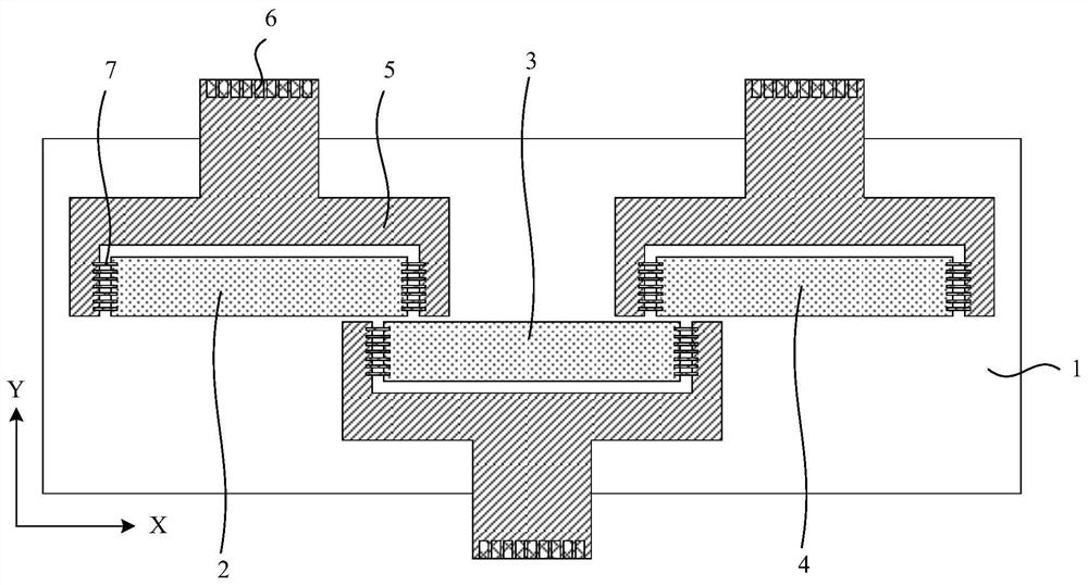
[0043] S2: Paste at least two print head chips sequentially on different positions on the upper surface of the base along the X direction, wherein the print head chip pasted in the later step and the print head chip pasted in the previous step are at least A part overlaps, the X direction and the Y direction are parallel to the upper surface of the base, and the X direction and the Y direction are perpendicular to each other.
[0044] As an example, see figure 1 , paste the three print head chips (the first print head chip 2, the second print head chip 3 and the third print head chip 4) on different positions on the upper surface of the base 1 in sequence along the X direction, wherein the last step is to paste The print head chip and the print head chip pasted in the previous step are at least partly ov...
Embodiment 2
[0057] This embodiment adopts basically the same technical solution as Embodiment 1, except that the material of the base is more optimized.
[0058] Specifically, before mounting the print head chip, the base needs to be cleaned and pre-baked after cleaning. When the base is made of plastic finishing parts, the measurement data shows that the base deforms sadly after baking, and the deformation is about 150 microns. Such as figure 2 As shown, the print head chip is a silicon-based material with good rigidity. When it is attached to the deformed base, the chip is uneven, which affects the accuracy of the chip position. A variety of plastic base materials are selected for testing, and all have different degrees of warpage.
[0059] In this embodiment, in order to achieve a deformation coefficient close to that of the print head chip material, a ceramic material is finally selected as the base. Among them, the CTE coefficient (thermal expansion coefficient) of ceramics is ab...
Embodiment 3
[0062] This embodiment adopts basically the same technical solution as Embodiment 1, except that the material of the base is more optimized, and a pre-curing step of glue is added.
[0063] Specifically, the print head chip is bonded with heat-curing glue, and the selected high-viscosity glue can prevent the chip from moving after mounting. The experiment found that the position of the chip did not move significantly after mounting, but when the chip was baked and cured in an oven at high temperature, the viscosity of the glue decreased at high temperature, and the glue reaction would cause a small displacement of the chip. Evaluating glues with different viscosities, it is still found that the chip has displacement phenomenon after baking.
[0064] In this embodiment, UV thermosetting glue is used (UV system raw materials are added to the thermosetting glue). Compared with ordinary UV glue that does not need heat curing, the UV thermosetting glue used in this embodiment is mo...
PUM
 Abstract
Description
Claims
Application Information


