Phase gradient metasurface antenna of microstrip-line-like feed structure

A technology of microstrip line feeding and phase gradient, which is applied in the direction of antenna grounding switch structure connection, antenna, antenna grounding device, etc., can solve the problem that the metasurface antenna cannot take into account low profile and high performance, and achieve high degree of freedom and enhanced Orientation, the effect of realizing the degree of freedom

Pending Publication Date: 2021-12-03
GUILIN UNIV OF ELECTRONIC TECH
0 Cites 1 Cited by

AI-Extracted Technical Summary

Problems solved by technology

[0003] What the present invention is to solve is the problem that the existing metasurface antenna cannot take into account both ...

Abstract

The invention discloses a phase gradient metasurface antenna of a microstrip-line-like feed structure. The phase gradient metasurface antenna is composed of the microstrip-line-like feed structure and a radiating body of a phase gradient metasurface. The microstrip line feed structure comprises an SMA coaxial connector, a rectangular waveguide, a horn waveguide and a similar microstrip line; wherein the similar microstrip line is composed of an upper metal strip, a lower metal plate and a metal connecting band. The radiating body of the phase gradient metasurface comprises more than two metamaterial units, a dielectric substrate and a metal ground. The antenna profile can be reduced, a feasible scheme is provided for the design of a low-profile antenna needing to generate any radiation beam in 5G communication network application, and the phase gradient metasurface is used for adjusting and controlling the direction of a directional diagram, so that the defects that a parabolic antenna is large in size and the feeding of an array antenna is complex can be overcome, and the advantage of high degree of freedom can be achieved.

Application Domain

Technology Topic

Dielectric substrateParabolic antenna +8

Image

  • Phase gradient metasurface antenna of microstrip-line-like feed structure
  • Phase gradient metasurface antenna of microstrip-line-like feed structure
  • Phase gradient metasurface antenna of microstrip-line-like feed structure

Examples

  • Experimental program(1)

Example Embodiment

[0028] In order to make the object, technical solution and advantages of the present invention clearer, the present invention will be further described in detail below in conjunction with specific examples.
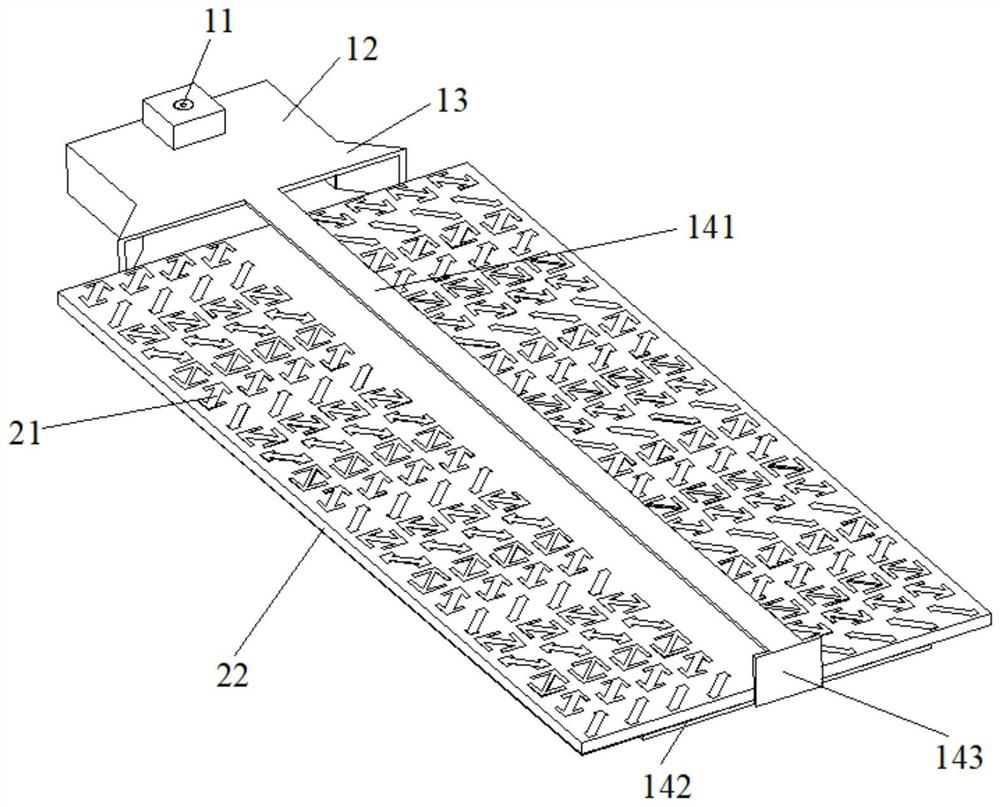
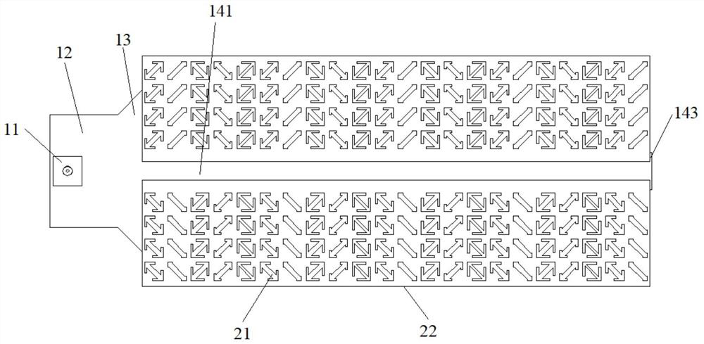
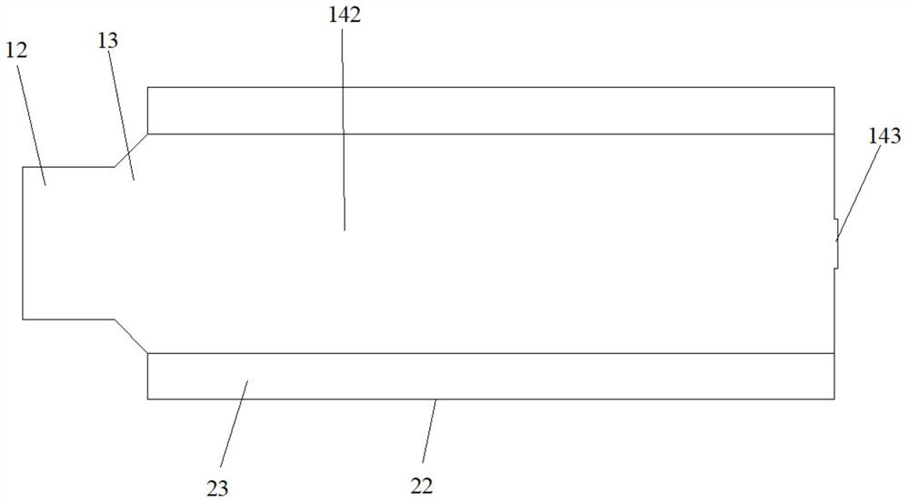
[0029] refer to Figure 1 to Figure 4 , a phase gradient metasurface antenna similar to a microstrip line feed structure, which consists of two parts: a microstrip line feed structure and a radiator of a phase gradient metasurface.
[0030] The microstrip-like feeding structure includes an SMA coaxial connector 11, a rectangular waveguide 12, a horn waveguide 13 and a similar microstrip line. The rectangular waveguide 12, the horn waveguide 13 and the quasi-microstrip line are all made of metallic copper. Both the rectangular waveguide 12 and the horn waveguide 13 are hollow cavity structures with closed upper and lower side walls and front and rear side walls. The left side wall of the rectangular waveguide 12 is closed, while the right side wall is opened. The left side wall and the right side wall of the horn waveguide 13 are openings, wherein the left side wall is a small opening surface, and the right side wall is a large opening surface. The opening shape and size of the right side wall of the rectangular waveguide 12 and the left side wall of the horn waveguide 13 are the same, and the right side wall of the rectangular waveguide 12 is connected with the opening edge of the left side wall of the horn waveguide 13 . The quasi-microstrip line is composed of an upper metal strip 141, a lower metal plate 142 and a metal connection strip 143, with air in between. The upper metal strip 141 and the lower metal plate 142 extend horizontally, and the metal connecting strip 143 extends vertically. The upper metal strip 141 is at the same level as the upper side walls of the rectangular waveguide 12 and the horn waveguide 13 , and the left end of the upper metal strip 141 is connected to the middle of the opening edge of the right wall of the horn waveguide 13 . The lower metal plate 142 is at the same level as the lower side walls of the rectangular waveguide 12 and the horn waveguide 13 , and the left end of the lower metal plate 142 is connected to the middle of the opening edge of the right wall of the horn waveguide 13 . The right end of the upper metal strip 141 is connected to the upper end of the metal connection strip 143 , and the lower end of the metal connection strip 143 is connected to the right end of the lower metal plate 142 . The SMA coaxial connector 11 is installed on the rectangular waveguide 12 , and the probe of the SMA coaxial connector 11 penetrates into the rectangular waveguide 12 .
[0031] The radiator of the phase gradient metasurface includes several groups of metamaterial units 21 , a dielectric substrate 22 and a metal ground 23 . The metamaterial unit 21 and metal ground 23 of the radiator of the phase gradient metasurface are metal copper film, and the dielectric substrate substrate 22 is FR4 glass fiber board. All metamaterial units 21 are covered on the upper surface of the dielectric substrate substrate 22, and are periodically arranged on the upper surface of the dielectric substrate substrate 22, and the metamaterial units 21 are arranged on both sides of the central axis of the narrow side of the dielectric substrate substrate 22. The sides are distributed symmetrically, so that the electromagnetic wave guided by the microstrip line can propagate to both sides, and excite the metamaterial units 21 on both sides. The metal ground 23 covers the lower surface of the dielectric substrate substrate 22 . Each group of metamaterial units 21 includes 5 unit structures, each unit structure is in the shape of a double-headed arrow, and the shapes and sizes of the 5 unit structures are different from each other. like Figure 5.
[0032] The radiator of the phase gradient metasurface is horizontally arranged between the upper metal strip 141 and the lower metal plate 142 of the similar microstrip line, and the metal ground 23 of the radiator of the phase gradient metasurface and the lower metal plate 142 of the similar microstrip line stick together. The width of the upper metal strip 141 is smaller than the width of the metal connecting strip 143 , and the width of the metal connecting strip 143 is smaller than the width of the lower metal plate 142 . The width of the lower metal plate 142 is equal to the maximum width of the lower sidewall of the horn waveguide 13 . The central axis of the narrow side of the upper metal strip 141, the lower metal plate 142 and the metal connection strip 143 of the microstrip line feeding structure is on the same vertical plane as the central axis of the narrow side of the dielectric substrate substrate 22 of the radiator of the phase gradient metasurface .
[0033] In this embodiment, the metal used in the microstrip-like feeding structure is copper with a conductivity of 58000000 s/m, and the thickness of the rectangular waveguide 12, the horn waveguide 13 and the microstrip-like line are all 1 mm. The SMA coaxial connector 11 feeds the rectangular waveguide 12. At this time, the mode is converted, and the TEM mode in the coaxial line is converted to TE 10mold. The radius of the probe of the SMA coaxial connector 11 is 0.62 mm, the radius of the metal shell of the SMA coaxial connector 11 is 2 mm, and the length of the probe of the SMA coaxial connector is optimized to be 16.2 mm. The rectangular waveguide 12 has a length of 29.4mm, a width of 49mm and a height of 12mm. Rectangular waveguide 12 TE 10 The mode electromagnetic wave guides and propagates to the horn waveguide 13, and the horn waveguide 13 is a deformation of the rectangular waveguide, changing the size of the opening makes the directional radiation propagation of the electromagnetic wave better. The length of the horn waveguide 13 is 10.6 mm, the width of the small opening is 49 mm, the width of the large opening is 70 mm, and the opening angle is 45°. The horn waveguide 13 is connected to a similar microstrip line. The width of the upper metal strip 141 of the microstrip line is 8 mm, the width of the lower metal plate 141 of the microstrip line is 70 mm, and the height of the metal connection strip 143 of the microstrip line is the height of the upper metal strip 141. The distance between the upper surface of the lower metal plate 141 is 10 mm, which is just enough to constrain the forward propagation of electromagnetic waves and at the same time reasonably excite the metasurface units.
[0034] In this embodiment, the radiator of the phase gradient metasurface is composed of two materials: metal copper and FR4 glass fiber plate. The dielectric substrate substrate 22 is made of FR4 glass fiber board with a dielectric constant of 4.4, a loss tangent of 0.02, a thickness of 3 mm, a length of 220 mm, and a width of 100 mm. The material of the metamaterial unit 21 and the metal ground 23 is metallic copper. For the five double-arrow-shaped unit structures of each group of metamaterial unit 21, the two ends of the double-headed arrows of the first, fourth and fifth unit structures point to the northeast and southwest directions respectively, and the second and third The two ends of the double arrow shape of the unit structure point to the southeast and northwest respectively. The radiator of the phase gradient metasurface has a total of 176 double-arrow-shaped unit structures, which are composed of five double-arrow-shaped unit structures of different sizes as a cycle, and the size of each double-arrow-shaped unit structure is 8mm× 8mm. Divide 176 unit structures in the shape of double arrows into two groups, two groups of metamaterial units 21 are distributed symmetrically to the central axis of the narrow side of the dielectric substrate substrate 22, and the distance between the two groups of metamaterial units 21 and the central axis of the narrow side of the dielectric substrate substrate 22 It is 9.6mm. This symmetrical distribution can easily realize the characteristics of dual beams. By changing the size of the double-arrow-shaped unit structure, the phase difference between the double-arrow-shaped unit structures can be changed, thereby changing the deflection of the pattern. Angle, and then synthesize the required pattern.
[0035] Image 6 and Figure 7 They are graphs of the cross-polarized reflection amplitude and phase of the metamaterial unit 21 with 5 double-arrow-shaped unit structures in the frequency range of 4GHz˜7GHz as a function of frequency. From the figure, we can see that the opening sizes of the five double-arrow-shaped unit structures are different, and the rotation directions are different, resulting in different phase characteristics of the five double-arrow-shaped unit structures. The phase difference is about 72°. Because of the existence of the metal ground 23, the amplitude characteristics of the five double-arrow-shaped unit structures are almost all greater than 0.8. Since the test environment of the amplitude-frequency characteristic curve and the phase-frequency characteristic curve is simulated by injecting electromagnetic waves vertically into the metamaterial unit 21, the actual measured frequency point needs to be higher than the originally required frequency band.
[0036] Figure 8 It is a graph of S11 varying with frequency in the frequency range of 3GHz to 7GHz in the present invention. It can be seen that the impedance bandwidth of the present invention is 4.65GHz-5.8GHz, and the relative bandwidth is about 22%. The applicable frequency band of the present invention covers one of the 5G frequency bands, and the resonance frequency of the present invention is 4.96GHz.
[0037] Figure 9-Figure 12 They are the E-plane radiation pattern and actual gain pattern at the four frequency points of the present invention at 4.7GHz, 4.8GHz, 4.9GHz and 5GHz, respectively. The deflection angles of the E-plane patterns at different frequency points are different, which shows that the antenna in this embodiment has weak frequency sweep characteristics, and the dual beams are more obvious at the two intermediate frequency points of 4.8GHz and 4.9GHz, and the maximum actual beam is at 5GHz. The gain reaches 11.4dBi.
[0038] It should be noted that although the above embodiments of the present invention are illustrative, they are not intended to limit the present invention, so the present invention is not limited to the above specific implementation manners. Without departing from the principles of the present invention, all other implementations obtained by those skilled in the art under the inspiration of the present invention are deemed to be within the protection of the present invention.

PUM

PropertyMeasurementUnit
Opening angle45.0deg
tensileMPa
Particle sizePa
strength10

Description & Claims & Application Information

We can also present the details of the Description, Claims and Application information to help users get a comprehensive understanding of the technical details of the patent, such as background art, summary of invention, brief description of drawings, description of embodiments, and other original content. On the other hand, users can also determine the specific scope of protection of the technology through the list of claims; as well as understand the changes in the life cycle of the technology with the presentation of the patent timeline. Login to view more.

Similar technology patents

Antenna

Owner:东莞市森岭智能科技有限公司

An antenna oscillator for a base station

PendingCN109244652AImprove Radiation PerformanceIncreased cross-polarization ratioRadiating elements structural formsAntennas earthing switches associationFeed lineCross polarization
Owner:深圳市鑫龙通信技术有限公司

AFU antenna

PendingCN114122702AImprove Radiation PerformanceAvoid Poor Antenna Performance StabilityRadiating elements structural formsRadiating element housingsRadomeBase station antennas
Owner:WUHAN HONGXIN TELECOMM TECH CO LTD

Classification and recommendation of technical efficacy words

  • High orientation
  • Improve Radiation Performance

Miboplatin liposome and preparation method thereof

InactiveCN103735509AHigh orientationReduce without damage or inhibitionPowder deliveryPharmaceutical product form changeLiposomeOil phase
Owner:SHANGHAI NEW ASIA PHARMA

High-efficiency denitration ionic liquid and application method thereof

ActiveCN109569240AHigh orientationReduce the degree of hydrolysisGas treatmentDispersed particle separationPeptideIon
Owner:山东汇之蓝环保科技有限公司

Rotating Electrical Machine

Owner:HITACHI ASTEMO LTD

Display Device

Owner:PANASONIC CORP

Metal frame mobile phone antenna

Owner:SHANGHAI AMPHENOL AIRWAVE COMM ELECTRONICS
Why Eureka
Try Eureka