SiC MOSFET device and preparation method thereof

A device and epitaxy technology, which is applied in the field of SiC MOSFET devices and its preparation, can solve problems such as gate oxide breakdown, achieve the effects of increasing breakdown voltage, not being easy to break down, and improving reliability

Pending Publication Date: 2021-12-21
深圳真茂佳半导体有限公司
View PDF0 Cites 0 Cited by
  • Summary
  • Abstract
  • Description
  • Claims
  • Application Information

AI Technical Summary

Problems solved by technology

[0005] In order to solve the problem of premature breakdown of the gate oxide of trench-type SiC MOSFET devices and improve the reliability of trench-type SiC MOSFET devices, the application provides a SiC MOSFET device and its preparation method

Method used


Image

  • SiC MOSFET device and preparation method thereof
  • SiC MOSFET device and preparation method thereof
  • SiC MOSFET device and preparation method thereof

Examples


Embodiment Construction

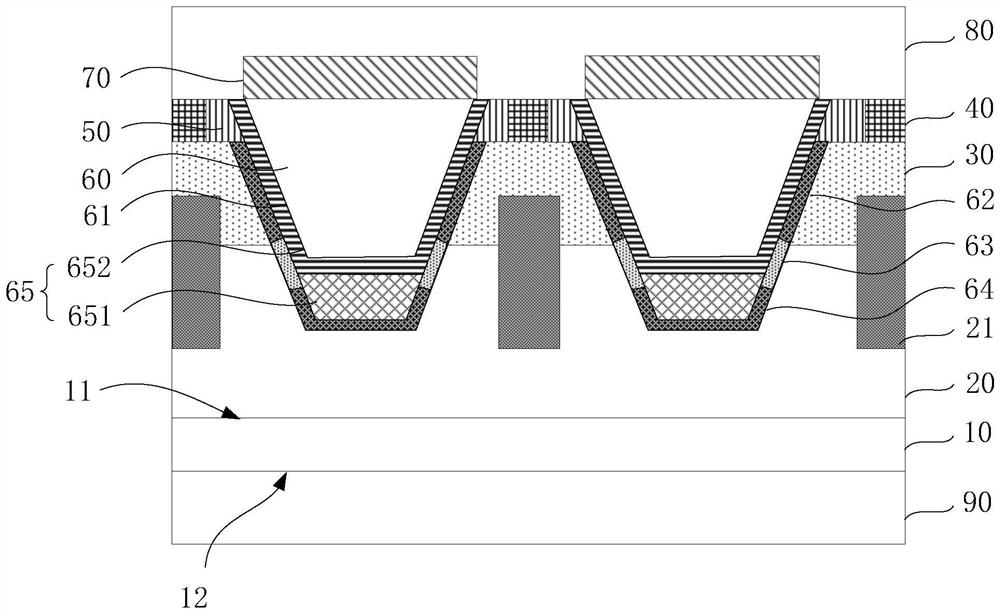
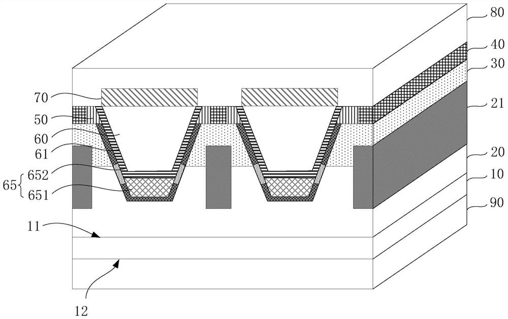
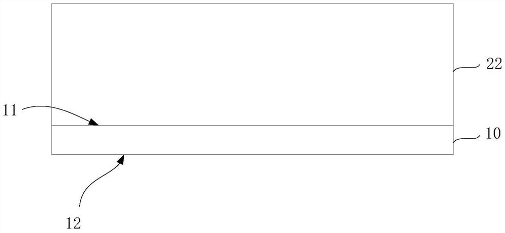
[0100] The technical solutions in the embodiments of the present application will be clearly and completely described below in conjunction with the accompanying drawings in the embodiments of the present application. Obviously, the described embodiments are only part of the embodiments for understanding the inventive concepts of the present application, and cannot represent All the embodiments are not explained as the only embodiment. Based on the embodiments in the present application, all other embodiments obtained by persons of ordinary skill in the art on the premise of understanding the inventive concepts of the present application fall within the protection scope of the present application.

[0101] It should be noted that if there is a directional indication (such as up, down, left, right, front, back...) in the embodiment of the present application, the directional indication is only used to explain the relationship between the components in a certain posture. If the s...


PUM

PropertyMeasurementUnit
thicknessaaaaaaaaaa
thicknessaaaaaaaaaa
thicknessaaaaaaaaaa

Abstract

The invention relates to the field of silicon carbide power devices, and discloses a SiC MOSFET device and a preparation method thereof. The SiC MOSFET device comprises a substrate, an epitaxial bottom layer, a base layer, a source layer, a gate, a gate dielectric layer, a protection layer, a channel section, a channel length reduction section, a floating section, an isolation layer, a source and a drain. The SiC MOSFET device is prepared based on the method comprising the steps of: forming the epitaxial bottom layer and the base layer on a first surface of the substrate, forming the protection layer in the epitaxial bottom layer and the base layer, forming the source layer and a base junction on the base layer, forming the gate, the gate dielectric layer, the channel section, the channel length reduction section and the floating section in a trench, forming an isolation layer on the gate layer, forming the source on the isolation layer and the source layer, and forming the drain on a second surface of the substrate. The gate dielectric layer is low in defect density, high in breakdown voltage and high in reliability.

Description

technical field [0001] The present application relates to the field of silicon carbide power devices, in particular to a SiC MOSFET device and a preparation method thereof. Background technique [0002] Because of its large band gap, high thermal conductivity, high breakdown field strength, high electron saturation rate and strong radiation resistance, silicon carbide power semiconductor devices can be used in high temperature, high pressure, high frequency and strong radiation working environments Down. [0003] Vertical MOSFETs mainly include planar double-injection MOSFETs and trench MOSFETs. Among them, the trench MOSFET device has no JFET area resistance and has a higher cell density, so it is considered to have a wider application prospect. [0004] However, in a trench MOSFET, the gate oxide is directly exposed to the drift region, and the electric field is concentrated at the corner of the gate oxide. The dielectric constant of SiC is SiO 2 2.5 times the dielectr...

Claims


Application Information

Patent Timeline
Patent Type & Authority Applications(China)
IPC IPC(8): H01L29/06H01L29/10H01L29/16H01L29/423H01L21/336H01L29/78
CPCH01L29/0615H01L29/1033H01L29/1608H01L29/4236H01L29/66068H01L29/7827
Inventor 任炜强春山正光谢文华杨正友
Owner 深圳真茂佳半导体有限公司
Why Eureka
Try Eureka