
Shield grid MOSFET and manufacturing method thereof

A technology of shielded gate and surface fabrication, used in semiconductor/solid-state device manufacturing, electrical components, circuits, etc., can solve problems such as slow response of shielded gate MOSFETs, increase distance, reduce gate-source capacitance, and reduce gate-drain capacitance. and the effect of gate-source capacitance

Active Publication Date: 2021-12-28
VANGUARD SEMICON CORP
View PDF10 Cites 3 Cited by
  • Summary
  • Abstract
  • Description
  • Claims
  • Application Information

AI Technical Summary

Problems solved by technology

[0003] In view of this, the application provides a shielded gate MOSFET and a manufacturing method to solve the problem that the existing shielded gate MOSFET has high The problem of slow response of the shielded gate MOSFET due to the gate-source capacitance

Method used


Image

  • Shield grid MOSFET and manufacturing method thereof
  • Shield grid MOSFET and manufacturing method thereof
  • Shield grid MOSFET and manufacturing method thereof

Examples


Embodiment Construction

[0034] The technical solution of the present application is described clearly and completely through the following examples. Obviously, the described examples are only some of the examples of the present application, not all of them. In the case of no conflict, the following embodiments and technical features thereof can be combined with each other.

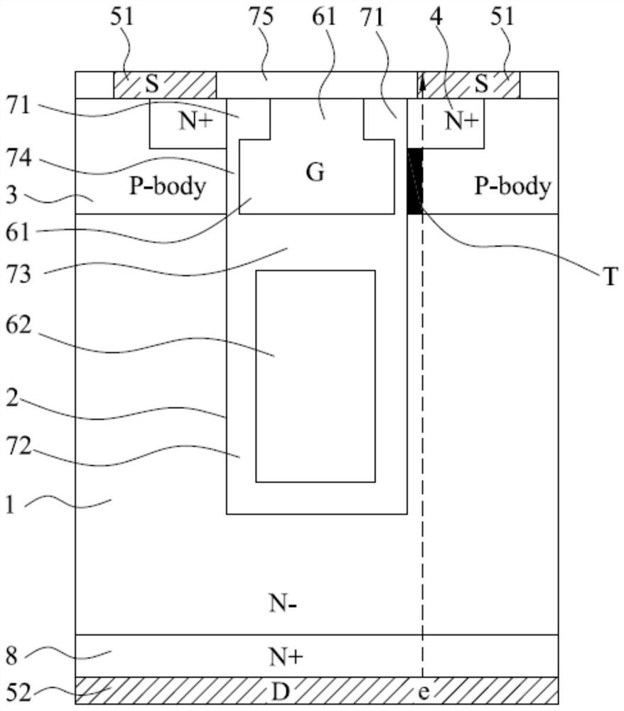
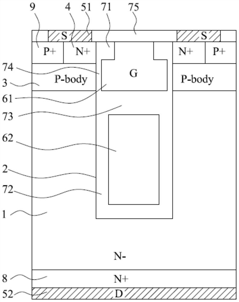
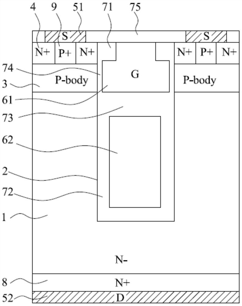
[0035] The embodiment of the present application provides a shielded gate MOSFET 100, such as figure 1 As shown, the shielded gate MOSFET 100 includes a drift region 1 of the first conductivity type, a trench 2 and a body region 3 of the second conductivity type, the trench 2 is located on the top of the drift region 1, and the body region 3 is located on both sides of the trench 2 side. It should be noted that, in some embodiments, the first conductivity type may be P-type conductivity, and correspondingly the second conductivity type may be N-type conductivity, or the first conductivity type may be N-type conductivity, and cor...


PUM


Abstract

The invention discloses a shield grid MOSFET and a manufacturing method thereof. The shield grid MOSFET comprises a drift region of a first conduction type, a trench located in the top of the drift region and body regions of a second conduction type located on the two sides of the trench; a grid electrode and a shield grid are arranged in the trench, the grid electrode is located above the shield grid, and a first doped region of a first conduction type is arranged on one side, close to the grid electrode, of the top of the body region; a source electrode is arranged on the top surface of the first doped region, and the body region is connected with the source electrode; the shield grid is connected with the source grid; and a first oxide layer is arranged between the grid electrode and the first doped region, a grid oxide layer is arranged between the grid electrode and the body region, a second oxide layer is arranged between the shield grid and the inner wall of the trench, a third oxide layer is arranged between the grid electrode and the shield grid, and the thickness of the first oxide layer is greater than that of the grid oxide layer. According to the shield grid MOSFET, the grid drain capacitance is reduced, the grid source capacitance is reduced, and the response speed of the shield gate MOSFET is improved.

Description

technical field [0001] The present application relates to the technical field of semiconductor devices, in particular to a shielded gate MOSFET and a manufacturing method thereof. Background technique [0002] The shielded gate MOSFET (Metal-Oxide-Semiconductor Field-Effect Transistor, MOSFET) introduces a shielded gate under the control gate to avoid direct contact between the control gate and the drift region, thus greatly reducing the gate-drain capacitance . However, since the shielding gate is connected to the source potential, a new gate-source capacitance will be generated between the control gate and the shielding gate, which will increase the gate-source capacitance and slow down the response of the shielded gate MOSFET. Contents of the invention [0003] In view of this, the present application provides a shielded gate MOSFET and a manufacturing method to solve the problem that the existing shielded gate MOSFET has a high gate-source capacitance after reducing t...

Claims


Application Information

Patent Timeline
IPC IPC(8): H01L29/06H01L29/423H01L29/78H01L21/336
CPCH01L29/0607H01L29/4236H01L29/7831H01L29/66484
Inventor 李伟聪姜春亮雷秀芳
Owner VANGUARD SEMICON CORP
Learn More