High-frequency sensor and manufacturing method thereof

A high-frequency sensor and sensor technology, applied in the field of sensors, can solve the problems of short time for returning echo signals, affecting the accuracy of ranging, and achieve the effects of improving accuracy, reducing cumbersome installation steps, and enhancing strength

Pending Publication Date: 2021-12-31
CHENGDU HUITONG WEST ELECTRONIC CO LTD
View PDF0 Cites 2 Cited by
  • Summary
  • Abstract
  • Description
  • Claims
  • Application Information

AI Technical Summary

Problems solved by technology

[0003] However, as the frequency increases, the time for the measured object to return the echo signal is shorter. In the extreme case, the aftershock of the ultrasonic sensor itself has not ended, the echo signal has arrived, and the aftershock and echo signal are superimposed. will affect the accuracy of distance measurement

Method used


Image

  • High-frequency sensor and manufacturing method thereof
  • High-frequency sensor and manufacturing method thereof
  • High-frequency sensor and manufacturing method thereof

Examples


Embodiment 1

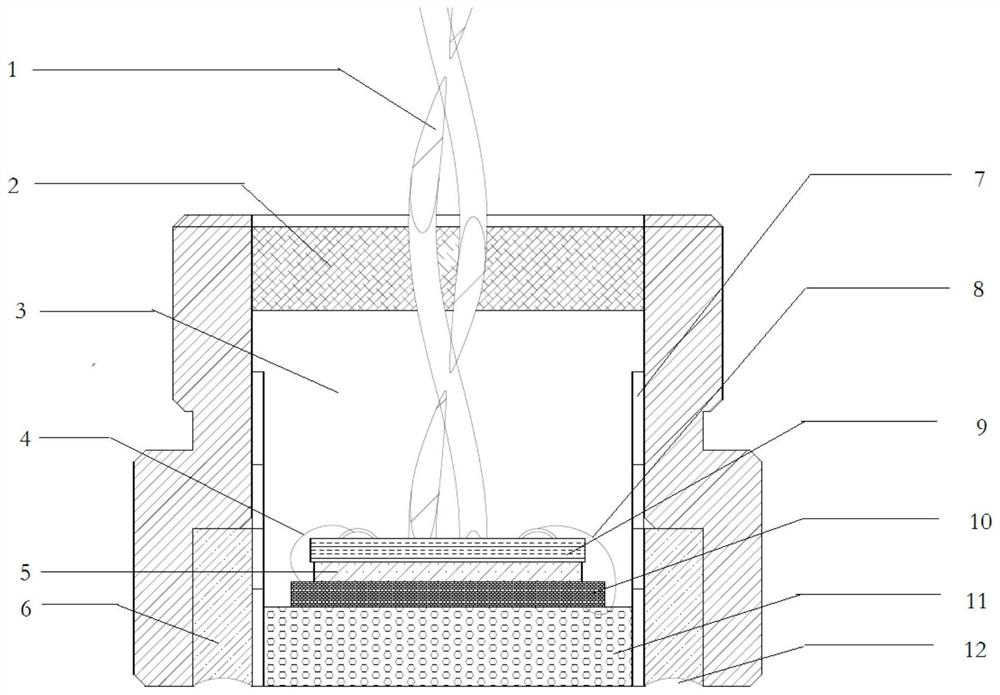
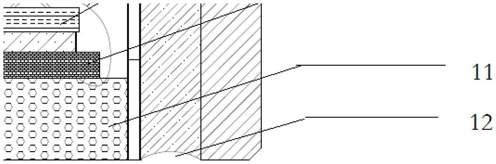
[0045] A high-frequency sensor, comprising a shell, a first matching layer, a PCB circuit board, a piezoelectric ceramic sheet and a second matching layer, the first matching layer, a PCB circuit board, a piezoelectric ceramic sheet and the second matching layer are arranged on the shell In the body, one side of the first matching layer is in contact with the housing, the other side of the first matching layer is in contact with the upper surface of the PCB circuit board, and the lower surface of the PCB circuit board is in contact with the upper surface of the piezoelectric ceramic sheet. The lower surface of the sheet is in close contact with the second matching layer, the other side of the second matching layer is used to transmit ultrasonic signals outward, and the connection between the other side of the second matching layer and the housing has an arc structure. The vibration-damping glue layer is also included, and the vibration-damping glue layer is arranged on the outs...

Embodiment 2

[0060] In the method for making a high-frequency sensor, the arc of the arc structure 12 is completed in the following manner:

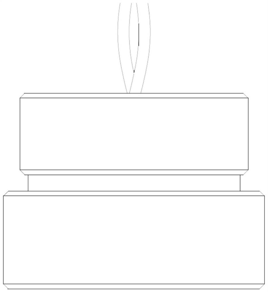
[0061] A) Put the semi-finished sensor with the glue injection side up into the dispensing tool, set the dispensing time and dispensing air pressure of the dispensing machine, and use the No. 6 needle in the glue layer on the side Apply a layer of primer first, and keep the glue between 3-5mm from the upper surface. The schematic diagram of the sensor placed with the glue injection side up is as follows: Figure 9 shown. The upper end surface refers to a plane that is flat with the surface of the second matching layer that is used to transmit ultrasonic signals to the outside.

[0062] B) Place the glued product in a 60-degree oven for 1 hour to dry;

[0063] C) Then apply a layer of glue on the entire surface of the product, keep the upper surface of the glue flat with the upper end surface, and then wipe off the excess glue. Or use the method o...


PUM


Abstract

The invention relates to the technical field of sensors, in particular to a high-frequency sensor and a manufacturing method thereof. The high-frequency sensor comprises a first matching layer, a PCB, a piezoelectric ceramic piece and a second matching layer which are arranged in a shell, wherein one face of the first matching layer is connected with the upper bottom face of the shell, and the other face of the first matching layer is connected with one face of the PCB; the other side of the PCB is connected with one side of the piezoelectric ceramic piece, the other side of the piezoelectric ceramic piece is connected with the second matching layer, and the other side of the second matching layer is used for transmitting ultrasonic signals outwards. The sensor further comprises a vibration reduction glue layer, the vibration reduction glue layer is arranged on the outer side of the second matching layer, and an arc structure is arranged on the vibration reduction glue layer. The invention further discloses a method for manufacturing the sensor with the arc-shaped structure. Due to the design of the arc-shaped structure, the emission sound pressure and the receiving sensitivity of the product are not influenced by forced clamping of the shell wall. The arc-shaped structure is easy to manufacture, simple in process, low in cost and less in time consumption.

Description

technical field [0001] The invention relates to the technical field of sensors, in particular to a high-frequency sensor and a manufacturing method thereof. Background technique [0002] The ultrasonic sensor sends out an ultrasonic signal of a certain frequency and receives the echo signal. Through the time difference between sending and receiving the signal, the distance between the object causing the signal reflection and the sensor is obtained. Therefore, this solution is often used in the field of artificial intelligence for foreign object detection or distance detection. Generally, the higher the ultrasonic frequency emitted by the sensor, the more beneficial it is to detect close-range objects, and the higher the sensitivity to close-range objects, the smart device can make corresponding processing faster. Therefore, the industry continues to increase the frequency of ultrasonic sensors. , to detect closer objects. [0003] However, as the frequency increases, the t...

Claims


Application Information

Patent Timeline
Patent Type & Authority Applications(China)
IPC IPC(8): G01S15/08G01S15/04
CPCG01S15/08G01S15/04
Inventor 阴伏星李佳张博蔡东孙云锴
Owner CHENGDU HUITONG WEST ELECTRONIC CO LTD
Why Eureka
Try Eureka