Optical field frequency multiplication sweep device based on electro-optical material optical waveguide

A technology of electro-optical materials and optical waveguides, applied in the fields of instruments, optics, nonlinear optics, etc., can solve the problems of low sweep frequency, high driving voltage, large device size, etc., and achieve the effect of reducing the modulation frequency

Active Publication Date: 2021-12-31
JINAN UNIVERSITY
View PDF9 Cites 0 Cited by
  • Summary
  • Abstract
  • Description
  • Claims
  • Application Information

AI Technical Summary

Problems solved by technology

However, the above-mentioned technologies or devices have defects such as high driving voltage, large device volume, light field deflection dependent on the wavelength of the light source, and low sweep frequency.

Method used


Image

  • Optical field frequency multiplication sweep device based on electro-optical material optical waveguide
  • Optical field frequency multiplication sweep device based on electro-optical material optical waveguide
  • Optical field frequency multiplication sweep device based on electro-optical material optical waveguide

Examples


Embodiment 1

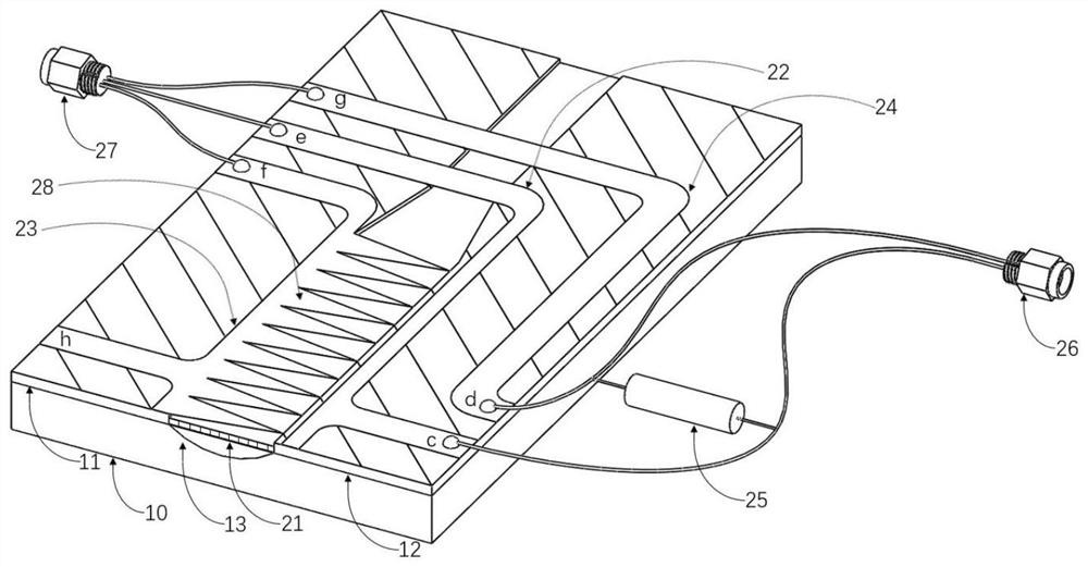
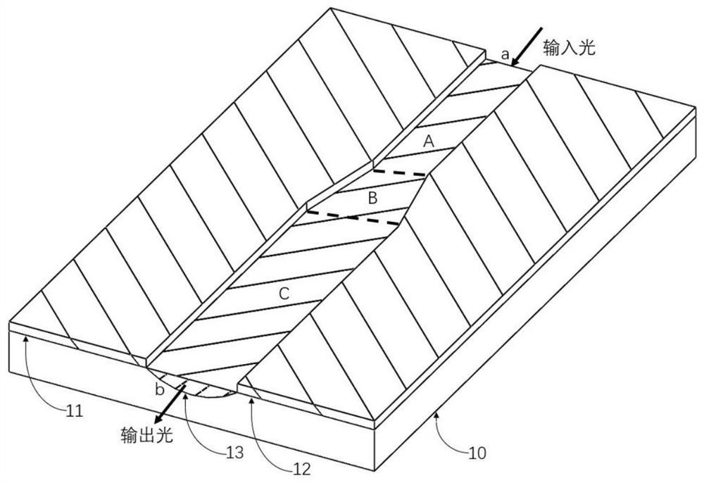
[0050] refer to figure 1 and figure 2 , the present invention provides an optical field frequency multiplication sweeper based on an electro-optic material optical waveguide, comprising a substrate 10, a first mask plate 11, a second mask plate 12, a waveguide core layer 13, and a waveguide core layer buffer layer 21. Sawtooth electrode, signal electrode 22 with double tentacles, ground electrode 23 with first double tentacles, ground electrode 24 with second double tentacles, matching resistor 25, first signal input port 26 and second signal input port 27:

[0051] The thicknesses of the first mask plate 11 and the second mask plate 12 are equal, and the first mask plate 11 and the second mask plate 12 are arranged at intervals on the substrate 10. The substrate 10, the first mask plate 12 The mask plate 11 and the second mask plate 12 form a groove-like space, the depth of the groove is the same as the thickness of the first mask plate 11 and the second mask plate 12, and th...

Embodiment 2

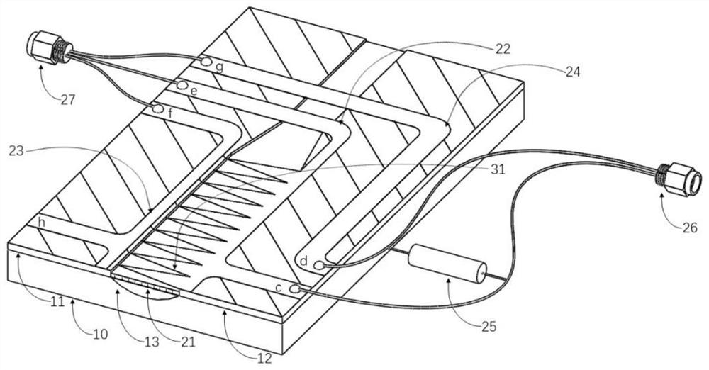
[0067] This embodiment is similar to Embodiment 1, refer to figure 2 and image 3 , is a schematic diagram of another scheme of the optical waveguide device. The difference between this embodiment and Embodiment 1 is that the bottom edge of the isosceles triangular sawtooth electrode 31 is connected to the double-antenna signal electrode 22, and the apex faces the first double-antenna ground wire electrode 23, and the height on the bottom side is equal to the width of the beam output area C of the waveguide core layer. The vertex of the isosceles triangular sawtooth electrode 31 is not in contact with the first double-stent ground electrode 22 , and its vertex is about 5 μm away from the first double-stent ground electrode 22 .

[0068] In the optical waveguide of the second embodiment, the refractive index of the waveguide core layer 13 is changed into a phased array by connecting the sawtooth electrode 31 of the double-tentacle signal electrode 22, thereby improving the de...

Embodiment 3

[0070] Such as Figure 4 Shown is a schematic diagram of an electro-optic and thermo-optic dual-effect mode wiggler experimental device, a laser 41, an input optical fiber 42, an optical waveguide 43, a signal source 44, a lens 45 and a mode monitor 46, wherein the input optical fiber 42 includes a single-mode optical fiber or a panda Polarization-maintaining fiber, preferably, Panda polarization-maintaining fiber is used as the input fiber 52 . The light beam to be adjusted outputted by the laser 41 is exported through the connection input optical fiber 42 . The tail end of the input optical fiber 42 is aligned with the center of the input end face a of the optical waveguide, so that the light beam to be modulated is coupled into the optical waveguide 43 . The signal input port of the optical waveguide is connected to the signal source 44, so that the light beam in the optical waveguide is modulated. If the signal source 44 is connected to the first signal input port on the ...


PUM

PropertyMeasurementUnit
lengthaaaaaaaaaa
widthaaaaaaaaaa
thicknessaaaaaaaaaa

Abstract

The invention discloses an optical field frequency multiplication sweep device based on an electro-optical material optical waveguide. The optical field frequency multiplication sweep device comprises a substrate, a first mask plate, a second mask plate, a waveguide core layer, a sawtooth electrode, a double-contact-pin signal electrode, a first double-contact-pin ground wire electrode, a second double-contact-pin ground wire electrode, a matched resistor, a first signal input port and a second signal input port. According to the invention, heat is generated when current passes through the double-contact-pin signal electrode, so that the thermo-optic effect of the waveguide core layer and the driving voltage and the phased array for controlling the periodic change of the refractive index in the core layer realize frequency doubling modulation of mode sweep, and the required modulation voltage and the modulation frequency of the required modulation signal are effectively reduced. The optical field frequency multiplication sweep device based on the electro-optical material optical waveguide can be widely applied to the field of optical waveguide devices.

Description

technical field [0001] The invention relates to the field of optical waveguide devices, in particular to an optical field frequency doubling swinger based on an electro-optic material optical waveguide. Background technique [0002] At present, using mechanical control technology, electronically controlled liquid crystal technology, acousto-optic effect, thermo-optic beam deflection technology, spectral dispersion sweep technology and large-aperture electro-optic crystal deflector and other technologies or devices, the deflection of light field mode and beam sweep can be realized. put. However, the above-mentioned technologies or devices have defects such as high driving voltage, large device volume, dependence of optical field deflection on the wavelength of the light source, and low sweep frequency. Contents of the invention [0003] In order to solve the above-mentioned technical problems, the object of the present invention is to reduce the required modulation voltage...

Claims


Application Information

Patent Timeline
Patent Type & Authority Applications(China)
IPC IPC(8): G02F1/03G02F1/035
CPCG02F1/0316G02F1/0305G02F1/0327G02F1/035
Inventor 钟永春陈哲卢惠辉朱文国
Owner JINAN UNIVERSITY
Why Eureka
Try Eureka