Efficient pcb layout method, device, device and computer-readable storage medium

A layout method and computer program technology, applied in computer-aided design, CAD circuit design, calculation, etc., can solve problems such as troublesome layout and low efficiency, and achieve the effect of improving PCB layout, increasing the scope of application, and facilitating retrieval and maintenance

Active Publication Date: 2022-04-26
SHENZHEN MINIEYE INNOVATION TECH CO LTD
View PDF10 Cites 0 Cited by
  • Summary
  • Abstract
  • Description
  • Claims
  • Application Information

AI Technical Summary

Problems solved by technology

[0003] To this end, the embodiments of the present application provide a high-efficiency PCB layout method, device, equipment, and computer-readable storage medium, which can solve the technical problems of cumbersome and low-efficiency existing PCB layouts. The specific technical solutions are as follows:

Method used


Image

  • Efficient pcb layout method, device, device and computer-readable storage medium
  • Efficient pcb layout method, device, device and computer-readable storage medium
  • Efficient pcb layout method, device, device and computer-readable storage medium

Examples


Embodiment Construction

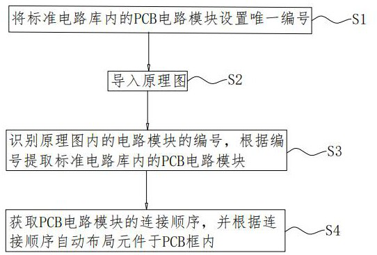
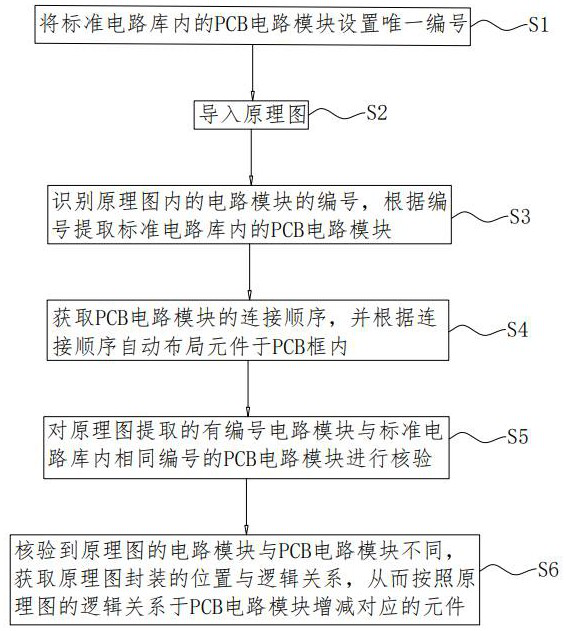
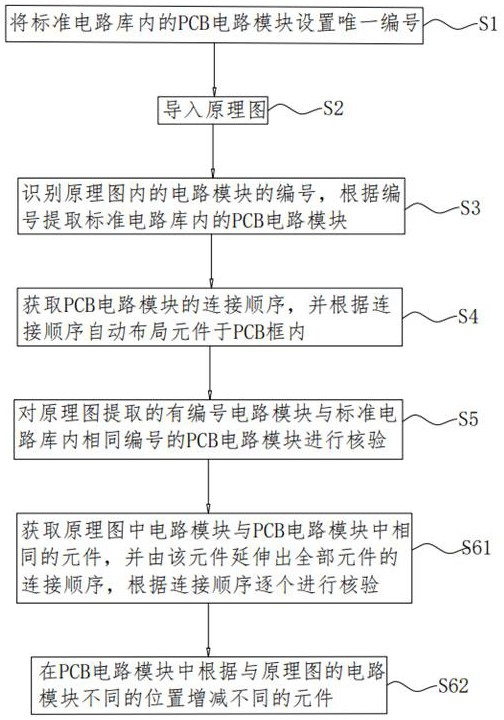
[0046] This specific embodiment is only an explanation of this application, and it is not a limitation of this application. Those skilled in the art can make modifications to this embodiment without creative contribution according to needs after reading this specification, but as long as the rights of this application All claims are protected by patent law.

[0047] In order to make the purposes, technical solutions and advantages of the embodiments of the present application clearer, the technical solutions in the embodiments of the present application will be clearly and completely described below in conjunction with the drawings in the embodiments of the present application. Obviously, the described embodiments It is a part of the embodiments of this application, not all of them. Based on the embodiments in this application, all other embodiments obtained by persons of ordinary skill in the art without creative efforts fall within the protection scope of this application. ...


PUM


Abstract

The present application relates to the technical field of PCB layout, in particular to an efficient PCB layout method, device, equipment and computer-readable storage medium. The method includes: setting a unique number for the PCB circuit module in the standard circuit library; importing the schematic diagram; identifying the serial number of the circuit module in the schematic diagram, and extracting the PCB circuit module in the standard circuit library according to the serial number; obtaining the connection sequence of the PCB circuit module , and automatically place components in the PCB frame according to the connection sequence. The present application solves the technical problems that the existing PCB layout is troublesome and inefficient.

Description

technical field [0001] The present application relates to the technical field of PCB layout, in particular to an efficient PCB layout method, device, equipment and computer-readable storage medium. Background technique [0002] At present, when laying out a normal PCB, it needs to rely on the schematic diagram and the PCB package library. When designing the layout, the designer manually imports the network connection relationship of the schematic diagram into the PCB file, and uses the package name from the PCB package library. Match the one-to-one corresponding PCB package, so as to complete the work of transferring the schematic netlist into the PCB file. At this time, the logical relationship between the position of all PCB packages and the schematic diagram is different, and it needs to be manually based on the logical relationship of the schematic diagram. Components are placed one by one, and each circuit is placed in a module layout. The layout effect may be different...

Claims


Application Information

Patent Timeline
Patent Type & Authority Patents(China)
IPC IPC(8): G06F30/392G06F30/398G06F115/12
CPCG06F30/392G06F30/398G06F2115/12
Inventor 辜民民刘国清杨广王启程聂晓楠
Owner SHENZHEN MINIEYE INNOVATION TECH CO LTD
Why Eureka
Try Eureka