Network matching structure display system of multi-stage design connection path
A connection path and network matching technology, applied in the field of electronics, can solve the problems of reducing design inspection efficiency, low display efficiency, and labor-intensive, etc., and achieve the effect of improving design inspection efficiency and wide utilization value.
- Summary
- Abstract
- Description
- Claims
- Application Information
AI Technical Summary
Problems solved by technology
Method used
Image

Examples
Embodiment Construction
[0015] In order to further explain the technical means and effects of the present invention to achieve the intended purpose of the invention, the following is a detailed description of a network matching structure display system with multi-level design connection paths proposed in accordance with the present invention in conjunction with the accompanying drawings and preferred embodiments. Embodiments and their effects are described in detail below.
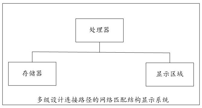
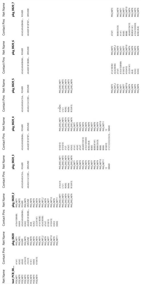
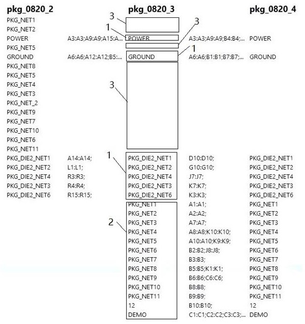
[0016] An embodiment of the present invention provides a network matching structure display system for multi-level design connection paths, such as figure 1 As shown, it includes a memory storing a computer program, a processor, and a display area, wherein, when the processor executes the computer program, it is used to respond to a network matching display creation instruction input by a user to obtain the multi-level design connection path The network matching parameters are displayed in the display area. It should be noted th...
PUM
 Abstract
Description
Claims
Application Information
 - Generate Ideas
- Intellectual Property
- Life Sciences
- Materials
- Tech Scout
- Unparalleled Data Quality
- Higher Quality Content
- 60% Fewer Hallucinations
Browse by: Latest US Patents, China's latest patents, Technical Efficacy Thesaurus, Application Domain, Technology Topic, Popular Technical Reports.
© 2025 PatSnap. All rights reserved.Legal|Privacy policy|Modern Slavery Act Transparency Statement|Sitemap|About US| Contact US: help@patsnap.com