
Artificial antiferromagnetic structure and memory element

A technology of artificial antiferromagnetic and antiferromagnetic layers, applied in the fields of information technology and spintronics

Pending Publication Date: 2022-01-21
SHANDONG UNIV
View PDF0 Cites 0 Cited by
  • Summary
  • Abstract
  • Description
  • Claims
  • Application Information

AI Technical Summary

Problems solved by technology

However, in order to realize deterministic magnetization switching caused by spin-orbit moment in the perpendicular anisotropic artificial antiferromagnetic structure with strong antiferromagnetic coupling, an auxiliary magnetic field up to 2000Oe to 10000Oe must be applied along the current direction, which becomes Bottleneck of strongly antiferromagnetically coupled perpendicularly anisotropic artificial antiferromagnetic structures in spintronic devices

Method used


Image

  • Artificial antiferromagnetic structure and memory element
  • Artificial antiferromagnetic structure and memory element
  • Artificial antiferromagnetic structure and memory element

Examples


Embodiment Construction

[0024] In order to have a clearer understanding of the technical features, purposes and effects of the present invention, the specific embodiments of the present invention will now be described with reference to the accompanying drawings, in which the same reference numerals represent components with the same or similar structures but the same functions.

[0025] In the following description, many specific details are set forth in order to fully understand the present invention. However, the present invention can also be implemented in other ways different from those described here. Therefore, the protection scope of the present invention is not limited by the specific details disclosed below. EXAMPLE LIMITATIONS.

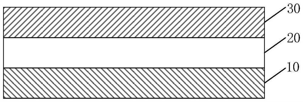
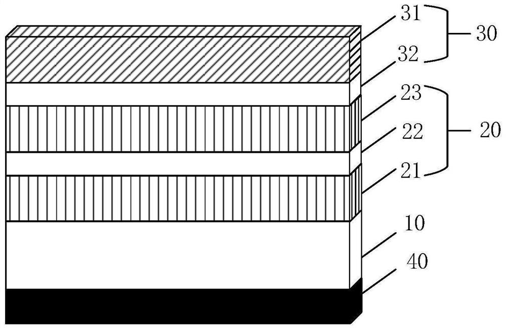
[0026] The embodiment of the present application provides an artificial antiferromagnetic structure, such as figure 1 As shown, can include:

[0027] The first metal layer 10, the artificial antiferromagnetic layer 20 and the second metal layer 30 are stacked in s...


PUM

PropertyMeasurementUnit
Thicknessaaaaaaaaaa

Abstract

The invention discloses an artificial antiferromagnetic structure and a memory element. The artificial antiferromagnetic structure comprises a first metal layer, an artificially synthesized antiferromagnetic layer and a second metal layer which are stacked in sequence, and an interface DM (Dzyaloshiski-Moriya) interaction exists between the metal layers and the artificially synthesized antiferromagnetic layer so that a first interface DM interaction exists between the first metal layer and the artificially synthesized antiferromagnetic layer, a second interface DM interaction exists between the second metal layer and the artificially synthesized antiferromagnetic layer, and the first interface DM interaction is different from the second interface DM interaction. The strong interface DM interaction enables the artificially synthesized antiferromagnetic layer to form a stable chiral Neel magnetic domain wall. And when the interaction of the first interface DM and the interaction of the second interface DM are different, the motion speeds of up-to-down and down-to-up magnetic domain walls in the chiral Neel magnetic domain wall can be obviously different through the current in a relatively small auxiliary magnetic field or even a zero magnetic field so that the deterministic magnetization overturning caused by the spin orbit moment is obtained.

Description

technical field [0001] The invention relates to the fields of information technology and spin electronics, in particular to an artificial antiferromagnetic structure and a storage element. Background technique [0002] The artificial antiferromagnetic structure refers to the interlayer exchange coupling between the two magnetic layers through the intermediate nonmagnetic layer, and the magnetic moments of the ferromagnetic layers are arranged in antiparallel under the action of the interlayer exchange coupling. Due to the strong exchange coupling between antiferromagnetic layers, the artificial antiferromagnetic structure has the advantages of small stray magnetic field and insensitivity to external magnetic field disturbance, etc., and is widely used as a pinning layer in a spin valve structure or a magnetic tunnel junction. It has greatly promoted the development of giant magnetoresistance and tunnel magnetoresistance devices. In recent years, with the discovery of novel ...

Claims


Application Information

Patent Timeline
IPC IPC(8): H01L43/02H01L43/08H01L27/22
CPCH10B61/10H10N50/80H10N50/10H10N50/85H01F10/3272H10B61/00H10N52/80H10N52/00
Inventor 颜世申田玉峰陈延学柏利慧周铁谢雪杰
Owner SHANDONG UNIV
Learn More