


Quick Research
Generate reliable direction feasibility study reports for your R&D in just a few steps.

Technical Q&A
Discover and master advanced knowledge NOW. Basics, ideas, possibilities, all at once.

Find Solutions
As an expert in R&D theories, this can generate solutions to your technical problems instantly.

Evaluate Feasibility
Analyze your overall solution with one click, know your potential R&D risks in advance.

Monitor Landscape
Get weekly tech updates, stay abreast of the latest tech innovations and key insights.
Method for rapidly improving perpendicular magnetic anisotropy
An anisotropic, perpendicular magnetic technology, applied in the manufacture/processing of magnetic field-controlled resistors, electromagnetic devices, etc., can solve problems such as high production costs and processes, and achieve good vertical magnetic anisotropy
- Summary
- Abstract
- Description
- Claims
- Application Information
AI Technical Summary
Problems solved by technology
Method used
Image

Examples
Embodiment 1
[0032] Thin Film Magnetic Heterojunction Material Ta(1nm) / Co 40 Fe 40 B 20 (0.5nm) / MgO(1nm) / Ta(1nm) is deposited at room temperature by magnetron sputtering equipment, the substrate is a silicon dioxide substrate (22mm×22mm), and the vacuum degree of the sputtering background is 3 ×10 -7 Torr, the working pressure of argon during the sputtering process was kept at 4.0×10 -3 Torr, Ta Target and Co 40 Fe 40 B 20 The target is DC sputtering, the sputtering current is 150mA and 100mA, the sputtering rate is 0.083nm / s and 0.049nm / s respectively, the MgO target is radio frequency sputtering, the sputtering voltage is 100W, and the sputtering rate is 0.02nm / s s;
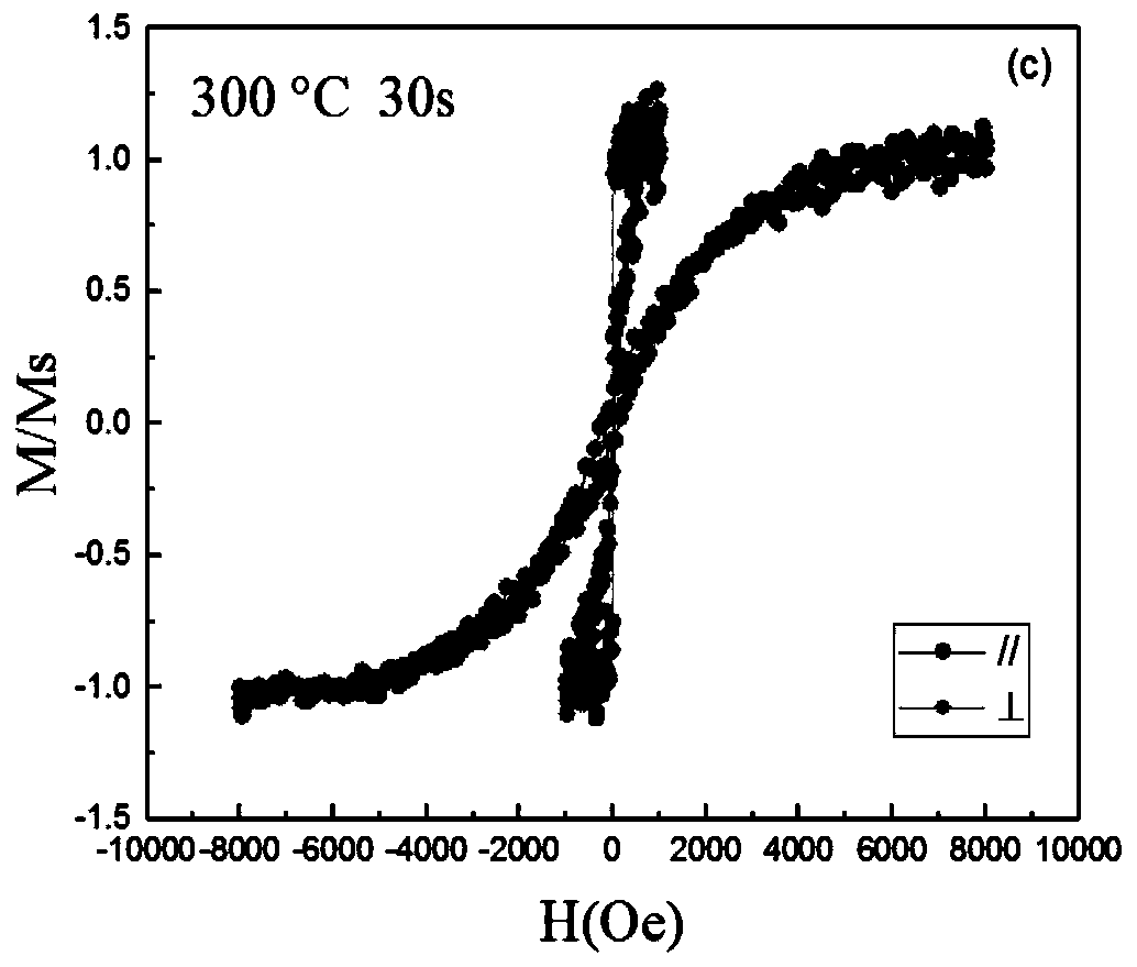
[0033] The purity of the targets used are all better than 99.99%. The sample heat treatment process is carried out in a vacuum annealing furnace. No external magnetic field is added during the annealing process. The annealing temperature is 300 ° C and the annealing time is 30s. Thin-film magnetic heterojunction mat...
Embodiment 2
[0048] Thin Film Magnetic Heterojunction Material Ta(2nm) / Co 40 Fe 40 B 20 (0.7nm) / MgO(1.2nm) / Ta(1.5nm) is deposited at room temperature by magnetron sputtering equipment, the substrate is a silicon dioxide substrate (22mm×22mm), the sputtering background vacuum 1×10 -7 Torr, the working pressure of argon during the sputtering process was kept at 4.0×10 -3 Torr, Ta Target and Co 40 Fe 40 B 20 The target is DC sputtering, the sputtering current is 150mA and 100mA, the sputtering rate is 0.083nm / s and 0.049nm / s respectively, the MgO target is radio frequency sputtering, the sputtering voltage is 100W, and the sputtering rate is 0.02nm / s s;
[0049] The purity of the targets used is better than 99.99%. The sample heat treatment process is carried out in a vacuum annealing furnace. No external magnetic field is added during the annealing process. Thin-film magnetic heterojunction materials.
Embodiment 3
[0051] Thin Film Magnetic Heterojunction Material Ta(3nm) / Co 40 Fe 40 B 20 (1nm) / MgO(1.5nm) / Ta(2nm) is deposited at room temperature by magnetron sputtering equipment, the substrate is a silicon dioxide substrate (22mm×22mm), and the vacuum degree of the sputtering background is 5 ×10 -7 Torr, the working pressure of argon during the sputtering process was kept at 4.0×10 -3 Torr, Ta Target and Co 40 Fe 40 B 20 The target is DC sputtering, the sputtering current is 150mA and 100mA, the sputtering rate is 0.083nm / s and 0.049nm / s respectively, the MgO target is radio frequency sputtering, the sputtering voltage is 100W, and the sputtering rate is 0.02nm / s s;
[0052] The purity of the targets used is better than 99.99%. The sample heat treatment process is carried out in a vacuum annealing furnace. No external magnetic field is added during the annealing process. The annealing temperature is 300 ° C and the annealing time is 50s. Thin-film magnetic heterojunction material...
PUM
 Abstract
Description
Claims
Application Information
 - R&D Engineer
- R&D Manager
- IP Professional
- Industry Leading Data Capabilities
- Powerful AI technology
- Patent DNA Extraction
Browse by: Latest US Patents, China's latest patents, Technical Efficacy Thesaurus, Application Domain, Technology Topic, Popular Technical Reports.
© 2024 PatSnap. All rights reserved.Legal|Privacy policy|Modern Slavery Act Transparency Statement|Sitemap|About US| Contact US: help@patsnap.com