


Quick Research
Generate reliable direction feasibility study reports for your R&D in just a few steps.

Technical Q&A
Discover and master advanced knowledge NOW. Basics, ideas, possibilities, all at once.

Find Solutions
As an expert in R&D theories, this can generate solutions to your technical problems instantly.

Evaluate Feasibility
Analyze your overall solution with one click, know your potential R&D risks in advance.

Monitor Landscape
Get weekly tech updates, stay abreast of the latest tech innovations and key insights.
A fast way to improve perpendicular magnetic anisotropy
An anisotropic, perpendicular magnetic technology, applied in the manufacture/processing of magnetic field-controlled resistors, electromagnetic devices, etc., can solve problems such as high production costs and processes, and achieve good vertical magnetic anisotropy
- Summary
- Abstract
- Description
- Claims
- Application Information
AI Technical Summary
Problems solved by technology
Method used
Image

Examples
Embodiment 1
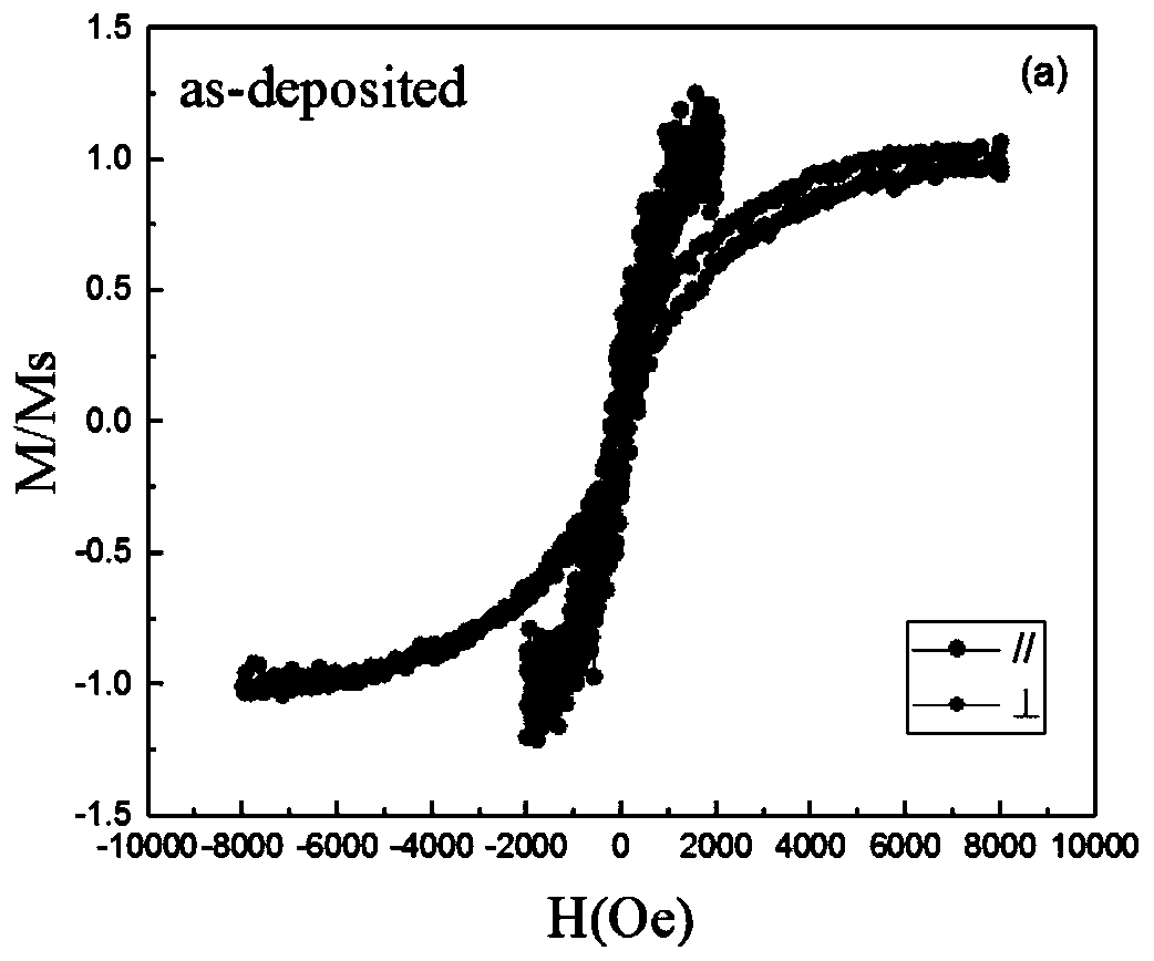
[0032] Thin Film Magnetic Heterojunction Material Ta(1nm) / Co 40 Fe 40 B 20 (0.5nm) / MgO(1nm) / Ta(1nm) is deposited at room temperature by magnetron sputtering equipment, the substrate is a silicon dioxide substrate (22mm×22mm), and the vacuum degree of the sputtering background is 3 ×10 -7 Torr, the working pressure of argon during the sputtering process was kept at 4.0×10 -3 Torr, Ta Target and Co 40 Fe 40 B 20 The target is DC sputtering, the sputtering current is 150mA and 100mA, the sputtering rate is 0.083nm / s and 0.049nm / s respectively, the MgO target is radio frequency sputtering, the sputtering voltage is 100W, and the sputtering rate is 0.02nm / s s;
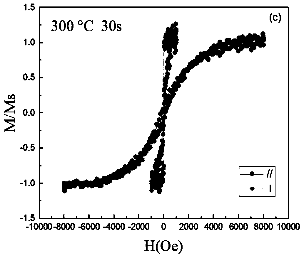
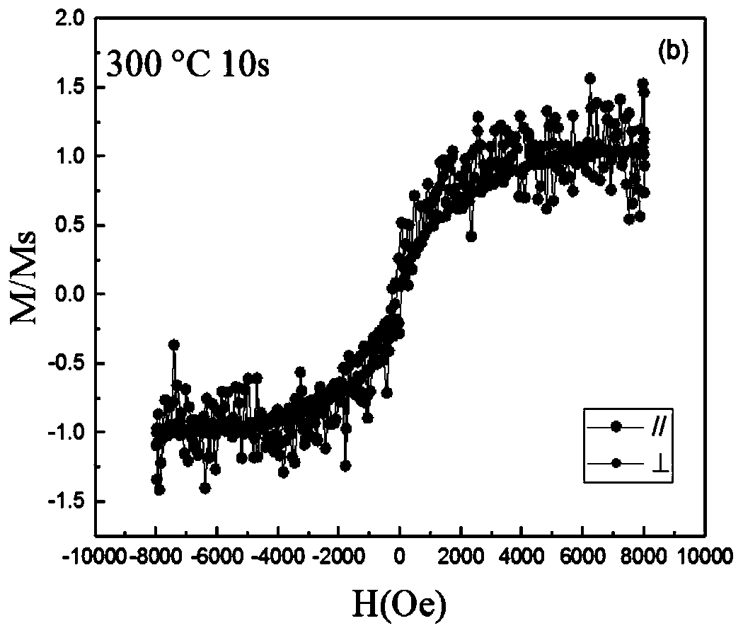
[0033] The purity of the targets used are all better than 99.99%. The sample heat treatment process is carried out in a vacuum annealing furnace. No external magnetic field is added during the annealing process. The annealing temperature is 300 ° C and the annealing time is 30s. Thin-film magnetic heterojunction mat...
Embodiment 2
[0048] Thin Film Magnetic Heterojunction Material Ta(2nm) / Co 40 Fe 40 B 20 (0.7nm) / MgO(1.2nm) / Ta(1.5nm) is deposited at room temperature by magnetron sputtering equipment, the substrate is a silicon dioxide substrate (22mm×22mm), the sputtering background vacuum 1×10 -7 Torr, the working pressure of argon during the sputtering process was kept at 4.0×10 -3 Torr, Ta Target and Co 40 Fe 40 B 20 The target is DC sputtering, the sputtering current is 150mA and 100mA, the sputtering rate is 0.083nm / s and 0.049nm / s respectively, the MgO target is radio frequency sputtering, the sputtering voltage is 100W, and the sputtering rate is 0.02nm / s s;
[0049] The purity of the targets used is better than 99.99%. The sample heat treatment process is carried out in a vacuum annealing furnace. No external magnetic field is added during the annealing process. Thin-film magnetic heterojunction materials.
Embodiment 3
[0051] Thin Film Magnetic Heterojunction Material Ta(3nm) / Co 40 Fe 40 B 20 (1nm) / MgO(1.5nm) / Ta(2nm) is deposited at room temperature by magnetron sputtering equipment, the substrate is a silicon dioxide substrate (22mm×22mm), and the vacuum degree of the sputtering background is 5 ×10 -7 Torr, the working pressure of argon during the sputtering process was kept at 4.0×10 -3 Torr, Ta Target and Co 40 Fe 40 B 20 The target is DC sputtering, the sputtering current is 150mA and 100mA, the sputtering rate is 0.083nm / s and 0.049nm / s respectively, the MgO target is radio frequency sputtering, the sputtering voltage is 100W, and the sputtering rate is 0.02nm / s s;
[0052] The purity of the targets used is better than 99.99%. The sample heat treatment process is carried out in a vacuum annealing furnace. No external magnetic field is added during the annealing process. The annealing temperature is 300 ° C and the annealing time is 50s. Thin-film magnetic heterojunction material...
PUM
 Abstract
Description
Claims
Application Information
 - R&D Engineer
- R&D Manager
- IP Professional
- Industry Leading Data Capabilities
- Powerful AI technology
- Patent DNA Extraction
Browse by: Latest US Patents, China's latest patents, Technical Efficacy Thesaurus, Application Domain, Technology Topic, Popular Technical Reports.
© 2024 PatSnap. All rights reserved.Legal|Privacy policy|Modern Slavery Act Transparency Statement|Sitemap|About US| Contact US: help@patsnap.com