PCB welding device

A technology for PCB circuit boards and welding devices, applied in auxiliary devices, printed circuits, welding equipment, etc., can solve the problems of increasing labor costs and inability to automate, and achieve the effects of improving work efficiency, stable spot welding, and convenient spot welding

Pending Publication Date: 2022-01-28
广德王氏智能电路科技有限公司
View PDF0 Cites 1 Cited by
  • Summary
  • Abstract
  • Description
  • Claims
  • Application Information

AI Technical Summary

Problems solved by technology

[0003] At present, during the electric welding process of the circuit board, the loading and unloading still needs to be carried out manually. After each electric welding is completed, the staff needs to disassemble and assemble the circuit board, which cannot realize complete automation and increases the labor cost.

Method used


Image

  • PCB welding device
  • PCB welding device
  • PCB welding device

Examples


Embodiment Construction

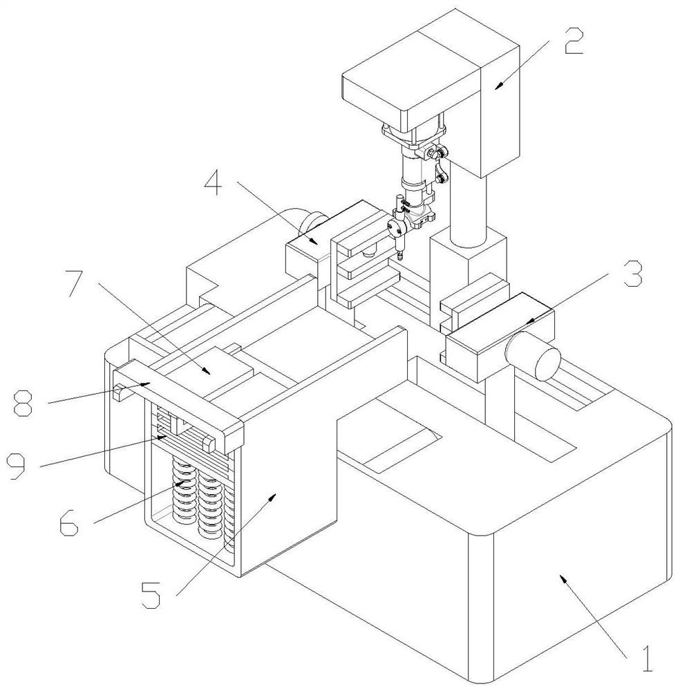
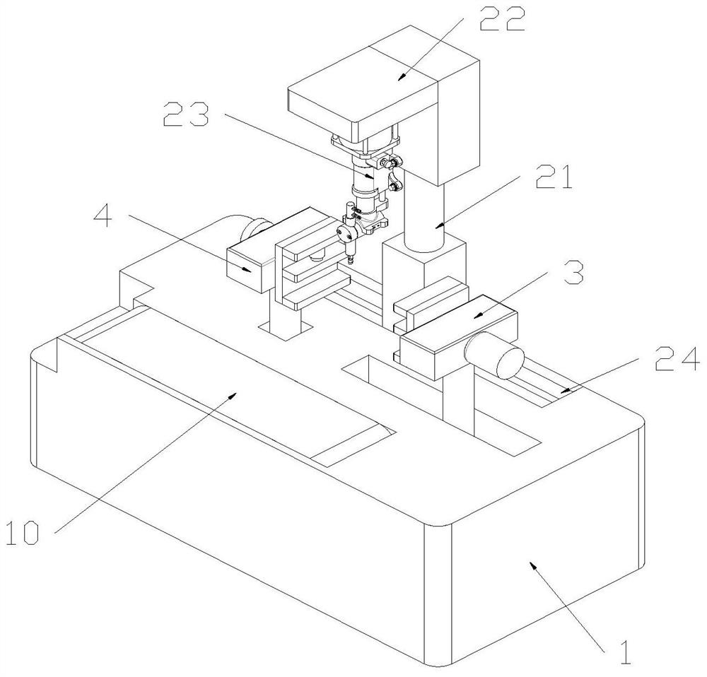
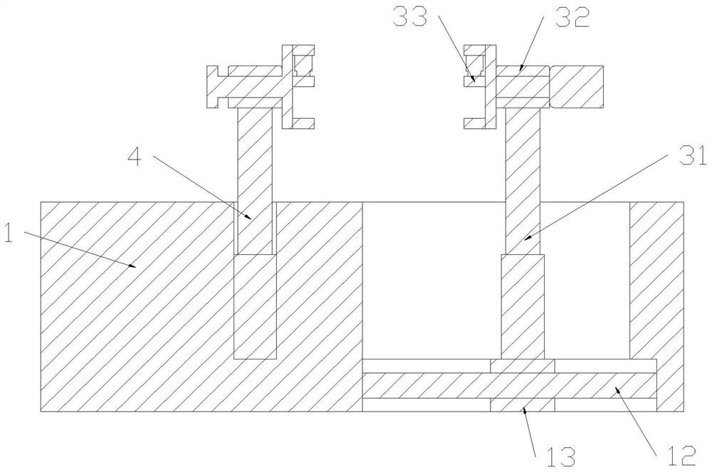
[0024] The following will clearly and completely describe the technical solutions in the embodiments of the present invention with reference to the accompanying drawings in the embodiments of the present invention. Obviously, the described embodiments are only some, not all, embodiments of the present invention. Based on the embodiments of the present invention, all other embodiments obtained by persons of ordinary skill in the art without creative efforts fall within the protection scope of the present invention.

[0025] In describing the present invention, it is to be understood that the terms "opening", "upper", "lower", "thickness", "top", "middle", "length", "inner", "surrounding" etc. Indicating orientation or positional relationship is only for the convenience of describing the present invention and simplifying the description, and does not indicate or imply that the components or elements referred to must have a specific orientation, be constructed and operated in a sp...


PUM


Abstract

The invention discloses a PCB (printed circuit board) welding device, which relates to the field of circuit board welding and comprises a worktable, a spot welding device is arranged on the surface of the worktable and movably connected with the worktable, a movable clamp is arranged at the front end of the spot welding device and slidably connected with the worktable, a fixed clamp is arranged at one side of the movable clamp, the fixed clamp is fixed to the surface of the worktable, the fixed clamp and the movable clamp are the same in structure, a feeding table is fixedly connected to the side wall of the worktable, a storage groove is formed in the rear end of the feeding table, and a lifting device is arranged in the storage groove. According to the invention, the feeding table is arranged, PCBs are stacked in the storage groove, the PCBs are pushed by a pushing device, the PCBs at the top are made to be tightly attached to a fixed baffle, then the PCBs at the uppermost end are pushed into the clamp through the pushing device to be clamped, and after spot welding, and the PCBs are attracted to a conveying belt through a traction plate and conveyed through the conveying belt; and operation is convenient and rapid, and manpower is not needed.

Description

technical field [0001] The invention relates to the field of circuit board welding, in particular to a PCB circuit board welding device. Background technique [0002] PCB soldering technology has developed in the electronics industry in recent years, and it can be noticed that an obvious trend is reflow soldering technology. In principle, traditional plug-in parts can also be used in reflow soldering process, which is commonly referred to as through-hole reflow soldering. The advantage is that it is possible to complete all solder joints at the same time, keeping production costs to a minimum. However, temperature-sensitive components limit the application of reflow soldering, whether it is a plug-in or an SMD. Then people turned their attention to selective welding. Selective soldering can be used after reflow soldering in most applications. This will be an economical and efficient soldering method for the remainder of the package and is fully compatible with future lea...

Claims


Application Information

Patent Timeline
Patent Type & Authority Applications(China)
IPC IPC(8): B23K37/00B23K37/047B23K101/42
CPCB23K37/00B23K37/047B23K2101/42
Inventor 王亚洲刘维李秀娟徐海峰
Owner 广德王氏智能电路科技有限公司
Why Eureka
Try Eureka