Manufacturing method of dielectric waveguide radio frequency device

A technology of radio-frequency devices and dielectric waveguides, which is applied to waveguide-type devices, electrical components, circuits, etc., can solve the problems that ceramic waveguide radio-frequency devices cannot be produced in large quantities, the performance of devices is reduced, and the processing efficiency is low, so as to achieve precision manufacturing and reduce the cost of devices. The effect of manufacturing difficulty and high processing precision

Active Publication Date: 2022-02-01
TIANJIN UNIV
View PDF6 Cites 3 Cited by
  • Summary
  • Abstract
  • Description
  • Claims
  • Application Information

AI Technical Summary

Problems solved by technology

[0007] The purpose of the present invention is to solve the problems of high cost, low processing efficiency, poor dimensional accuracy and poor surface quality of the existing method for preparing ceramic waveguide radio frequency devices, resulting in reduced device performance and inability to prepare ceramic waveguide radio frequency devices in large quantities, and to provide a A kind of manufacturing method of dielectric waveguide radio frequency device

Method used


Image

  • Manufacturing method of dielectric waveguide radio frequency device
  • Manufacturing method of dielectric waveguide radio frequency device
  • Manufacturing method of dielectric waveguide radio frequency device

Examples


specific Embodiment approach 1

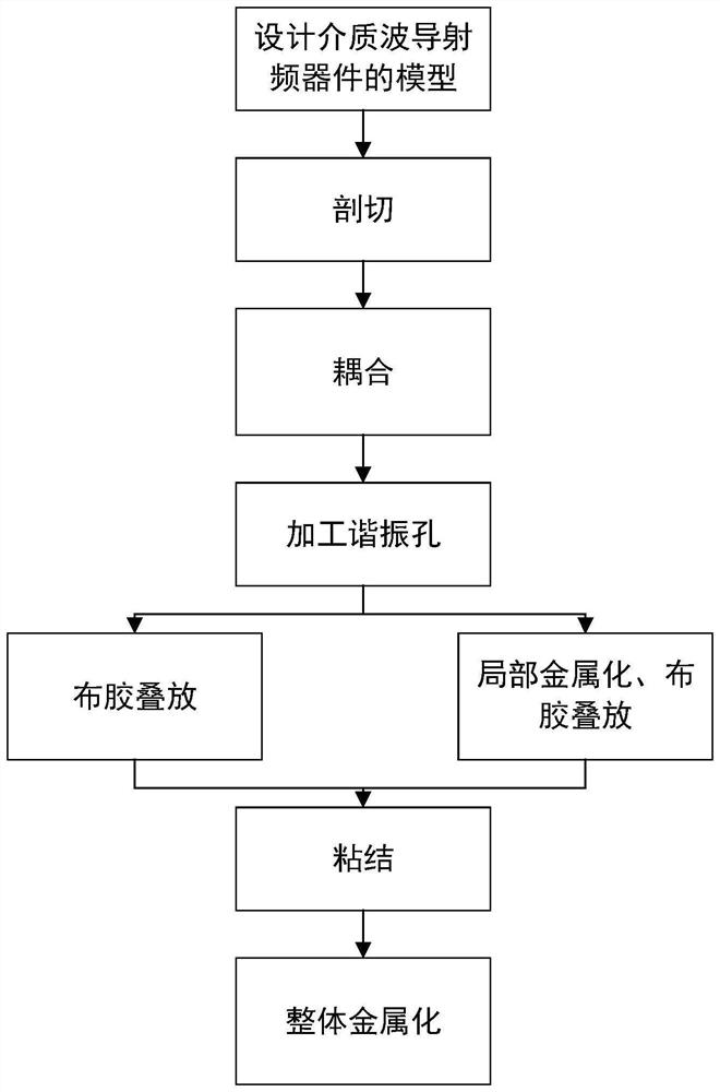
[0041] Specific Embodiment 1: In this embodiment, a method for manufacturing a dielectric waveguide radio frequency device is completed according to the following steps:

[0042] 1. Sectioning:

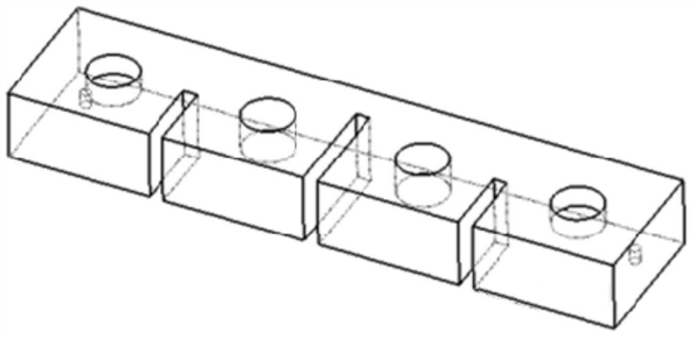
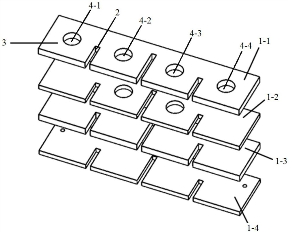
[0043] Design a dielectric waveguide radio frequency device, cut the dielectric material into n layers along one direction according to the model of the dielectric waveguide radio frequency device, and then grind, polish, and cut to obtain n layers of dielectric material sheets; n layers of dielectric material sheets from bottom to top stack settings;

[0044] 2. Coupling:

[0045] Determine the number of dielectric resonant cavities according to the design requirements of dielectric waveguide radio frequency devices, carry out coupling design between adjacent dielectric resonant cavities, and then process coupling structures on the corresponding layers of n-layer dielectric material sheets;

[0046] The coupling structure described in step 2 is slot coupling, through-hole coupling,...

specific Embodiment approach 2

[0063] Embodiment 2: The difference between this embodiment and Embodiment 1 is that the thicknesses of the n-layer dielectric material sheets described in Step 1 are the same or different. Other steps are the same as in the first embodiment.

specific Embodiment approach 3

[0064] Embodiment 3: This embodiment differs from Embodiment 1 or Embodiment 2 in that: the value range of n mentioned in Step 1 is 2≤n≤100. Other steps are the same as those in Embodiment 1 or 2.


PUM

PropertyMeasurementUnit
thicknessaaaaaaaaaa
thicknessaaaaaaaaaa
thicknessaaaaaaaaaa

Abstract

The invention discloses a manufacturing method of a dielectric waveguide radio frequency device, and relates to a manufacturing method of a waveguide radio frequency device. The invention aims to solve the problems that the existing method for preparing the ceramic waveguide radio frequency device is high in cost, low in processing efficiency, poor in size precision and poor in surface quality, so that the performance of the device is reduced, and the ceramic waveguide radio frequency device cannot be prepared on a large scale. The method comprises the following steps: 1, carrying out sectioning; 2, carrying out slotting; 3, processing tuning holes; 4, machining an energy input hole; 5, carrying out glue spreading and stacking; 6, carrying out bonding; and 7, carrying out overall metallization to obtain the dielectric waveguide radio frequency device. According to the invention, more complex and diversified device topological structure manufacturing can be realized, the device manufacturing difficulty is reduced, and the precision margin is improved; the processing precision is high, the process stability is good, and precise manufacturing of a subminiature dielectric waveguide radio frequency device can be realized, so that high frequency of the device is realized. According to the invention, the dielectric waveguide radio frequency device can be obtained.

Description

technical field [0001] The invention relates to a manufacturing method of a waveguide radio frequency device. Background technique [0002] Waveguide RF devices use the propagation and coupling of electromagnetic waves in the radio frequency band in the waveguide cavity to realize the transmission and processing of electromagnetic waves, mainly including waveguides, waveguide filters, waveguide multiplexers, waveguide antennas, etc. Compared with the air dielectric waveguide, the dielectric part of the waveguide is made of ceramic material, and the high dielectric constant of the ceramic can be used to adjust (generally reduce) the size of the device and realize the integration of the device. [0003] Conventional ceramic waveguide RF devices use ceramic powder to sinter into blanks and then perform precision machining, which results in high cost, low processing efficiency, and poor dimensional accuracy, resulting in reduced device performance. [0004] High-temperature co-...

Claims


Application Information

Patent Timeline
Patent Type & Authority Applications(China)
IPC IPC(8): H01P11/00
CPCH01P11/006
Inventor 林彬侯贺天王皓吉隋天一
Owner TIANJIN UNIV
Why Eureka
Try Eureka