Compensation method and compensation device for display panel

A technology of a display panel and a compensation method, which is applied to static indicators, instruments, etc., can solve the problems of wasting module repair and compensation capacity, affecting the pass-through rate of the module, and affecting the detection of the threshold voltage of surrounding sub-pixels.

Pending Publication Date: 2022-02-11
HUIZHOU CHINA STAR OPTOELECTRONICS TECHNOLOGY CO LTD +1
View PDF9 Cites 2 Cited by
  • Summary
  • Abstract
  • Description
  • Claims
  • Application Information

AI Technical Summary

Problems solved by technology

When a sub-pixel is defective due to the thin-film transistor process or the organic light-emitting layer process, it will affect the detection of the threshold voltage of the surrounding sub-pixels that share the detection circuit, causing the surrounding pixels to become bright or dark after being detected a

Method used


Image

  • Compensation method and compensation device for display panel
  • Compensation method and compensation device for display panel
  • Compensation method and compensation device for display panel

Examples


Embodiment Construction

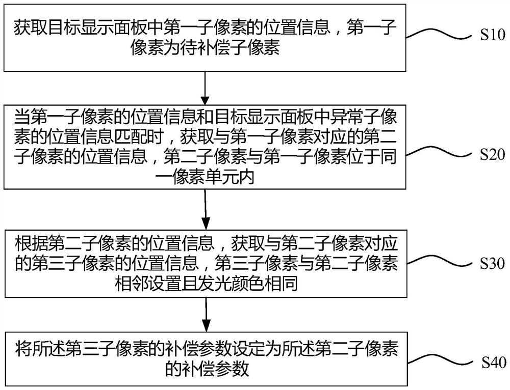
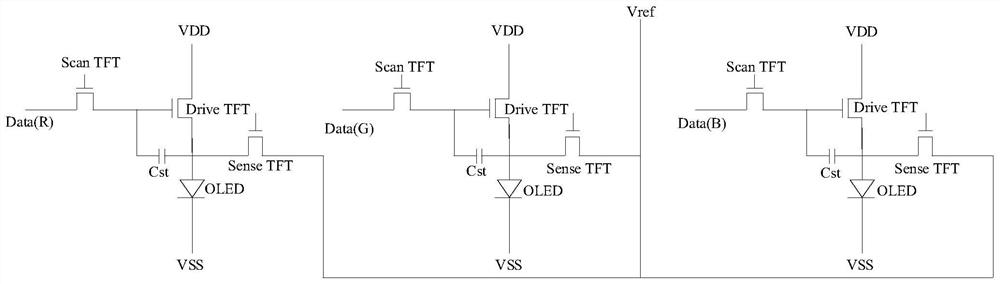
[0042] The following will clearly and completely describe the technical solutions in the embodiments of the application with reference to the drawings in the embodiments of the application. Apparently, the described embodiments are only some, not all, embodiments of the application. Based on the embodiments in this application, all other embodiments obtained by those skilled in the art without making creative efforts belong to the scope of protection of this application. In addition, it should be understood that the specific implementations described here are only used to illustrate and explain the present application, and are not intended to limit the present application. In this application, unless stated to the contrary, the used orientation words such as "up" and "down" usually refer to up and down in the actual use or working state of the device, specifically the direction of the drawing in the drawings ; while "inside" and "outside" refer to the outline of the device.

...


PUM


Abstract

The embodiment of the invention provides a compensation method and a compensation device for a display panel. The compensation method comprises the following steps: firstly, acquiring position information of a first sub-pixel; when the position information of the first sub-pixel is matched with the position information of the abnormal sub-pixel, obtaining the position information of a second sub-pixel, and the second sub-pixel and the first sub-pixel are located in the same pixel unit; then, according to the position information of the second sub-pixel, obtaining the position information of a third sub-pixel, and the third sub-pixel and the second sub-pixel are adjacently arranged and have the same light emitting color; and finally, setting the compensation parameter of the third sub-pixel as the compensation parameter of the second sub-pixel. According to the compensation method, whether display of the first sub-pixel is abnormal is determined firstly, then the compensation parameter of the third sub-pixel is set as the compensation parameter of the second sub-pixel, and therefore the situation that the second sub-pixel is compensated to be a bright spot or a dark spot due to the fact that the first sub-pixel has defects is avoided, the display module manufacturing process flow is optimized, and the repair and compensation capacity of the display module is reduced.

Description

technical field [0001] The present application relates to the display field, in particular to a compensation method and compensation device for a display panel. Background technique [0002] Different from Liquid Crystal Display (LCD for short) which uses a stable voltage to control brightness, Organic Light-Emitting Diode (OLED for short) is driven by current and requires a stable current to control light emission. Generally, an OLED display outputs current to the OLED through a driving transistor in a pixel driving circuit in each pixel, so as to drive the OLED to emit light. Due to the inconsistent electrical characteristics of the driving transistors in the OLED display, there are brightness differences between pixel units. In order to ensure the technical problem of inconsistency in brightness caused by the inconsistency of the electrical characteristics of the driving transistors, an external compensation method is proposed in the prior art. By compensating the thresh...

Claims


Application Information

Patent Timeline
IPC IPC(8): G09G3/3233G09G3/20
CPCG09G3/3233G09G3/2074G09G2320/043G09G2320/045
Inventor 何伟
Owner HUIZHOU CHINA STAR OPTOELECTRONICS TECHNOLOGY CO LTD
Why Eureka
Try Eureka