Error correction decoding method, storage medium and ssd device of nand flash memory chip

A flash memory chip and decoding technology, which is applied in the fields of error correction decoding, storage media and SSD equipment, can solve problems such as performance degradation and limited number of reads and writes, so as to improve the success rate, improve error correction ability, and reduce the number of attempts Effect

Active Publication Date: 2022-06-17
DERA CO LTD
View PDF2 Cites 0 Cited by
  • Summary
  • Abstract
  • Description
  • Claims
  • Application Information

AI Technical Summary

Problems solved by technology

[0002] NAND flash memory chips are widely used in the storage field due to their advantages such as large storage density, low power consumption, compatibility with silicon technology, good polymorphic characteristics, and non-volatility. lead to performance degradation in the later period of use

Method used


Image

  • Error correction decoding method, storage medium and ssd device of nand flash memory chip
  • Error correction decoding method, storage medium and ssd device of nand flash memory chip
  • Error correction decoding method, storage medium and ssd device of nand flash memory chip

Examples


Embodiment 1

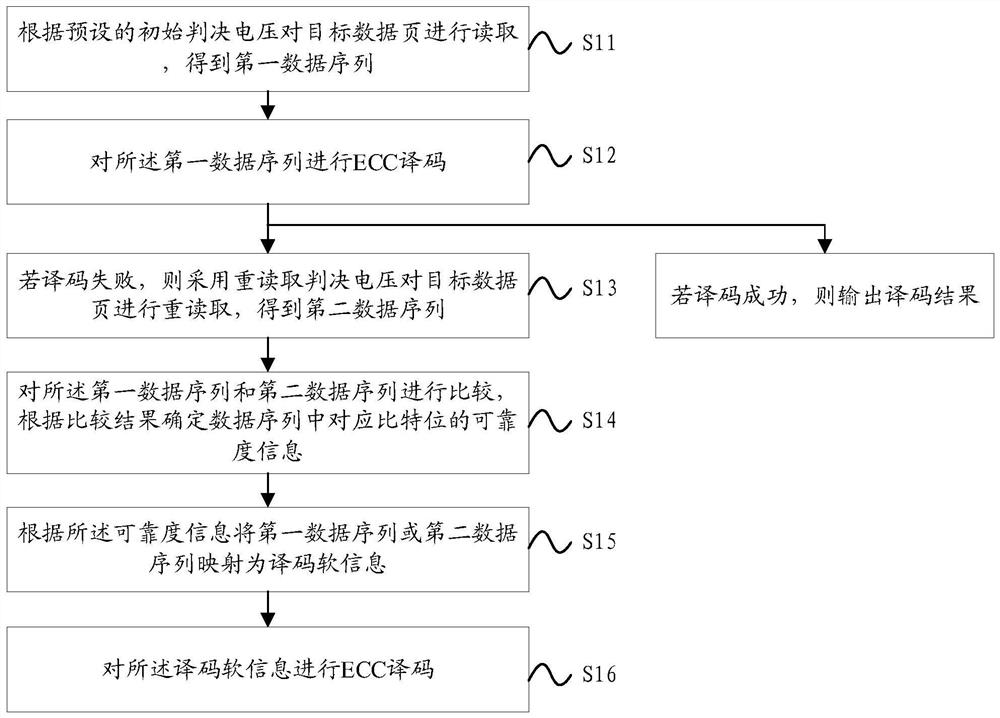
[0058] figure 1 A flowchart of an error correction decoding method for a NAND flash memory chip according to an embodiment of the present invention is schematically shown. refer to figure 1 , the error correction decoding method of the NAND flash memory chip according to the embodiment of the present invention specifically includes the following steps:

[0059] S11. Read the target data page according to the preset initial decision voltage to obtain a first data sequence.

[0060] The basic storage unit of a NAND flash memory chip is a data page (Page), and the effective capacity of each page is a multiple of 512 bytes. An SSD disk usually includes multiple NAND flash memory chips, and their operations are realized through SSD control.

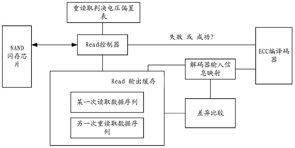
[0061] Read controller is a component of SSD controller like figure 2 As shown, the Read controller is responsible for reading data from the target data page of the NAND flash memory chip. Each read needs to configure the threshold volta...

Embodiment 2

[0115] Embodiments of the present invention further provide a computer-readable storage medium, on which a computer program is stored, and when the program is executed by a processor, implements the steps of the above error correction decoding method for a NAND flash memory chip.

Embodiment 3

[0117] An embodiment of the present invention further provides an SSD device, the SSD device includes a storage controller, the storage controller includes a memory, a processor, and a computer program stored in the memory and executable on the processor, the processor When the program is executed, the steps of the above error correction decoding method of the NAND flash memory chip are realized. E.g figure 1 S11 to S16 shown.

[0118] In the specific implementation process of the second embodiment to the third embodiment, reference may be made to the first embodiment, which has corresponding technical effects.


PUM


Abstract

The present invention provides an error correction decoding method for a NAND flash memory chip, a storage medium, and an SSD device. The method includes: reading a target data page according to a preset initial decision voltage to obtain a first data sequence; ECC decoding is performed on the first data sequence; if the decoding fails, the target data page is re-read using the re-read decision voltage to obtain a second data sequence; the first data sequence and the second data The sequences are compared, and the reliability information of corresponding bits in the data sequence is determined according to the comparison result; the first data sequence or the second data sequence is mapped into decoding soft information according to the reliability information; and the decoding soft information is performed ECC decoding. The error correction decoding method for the NAND flash memory chip, the storage medium and the SSD device proposed by the present invention can significantly improve the error correction capability of the ECC decoder and reduce the number of Read Retry attempts.

Description

technical field [0001] The present invention relates to the technical field of data storage, in particular to an error correction decoding method of a NAND flash memory chip, a storage medium and an SSD device. Background technique [0002] NAND flash memory chips have been widely used in the storage field due to their advantages of large storage density, storage capacity, low power consumption, compatibility with silicon technology, good polymorphism, and non-volatility. This results in lower performance later in use. Usually, a read retry error correction mechanism is provided inside the NAND flash memory chip. When the read data page in the NAND has an uncorrectable read error by the ECC (error control coding, error correction code) codec, it tries to deviate from the normal The threshold voltage method finds the closest ideal threshold voltage and tries to read the data correctly. [0003] In the data read by the threshold voltage of the Read Retry attempt, each data h...

Claims


Application Information

Patent Timeline
Patent Type & Authority Patents(China)
IPC IPC(8): G11C29/42G06F11/10
CPCG11C29/42G06F11/1012G06F11/1068
Inventor 秦东润刘晓健王嵩
Owner DERA CO LTD
Why Eureka
Try Eureka