Chip laminating equipment

A technology for laminating equipment and chips, which is applied in the direction of electrical components, semiconductor/solid-state device manufacturing, circuits, etc., can solve the problems of high cost, low production efficiency, low pass rate of chip attachment, etc., achieve high productivity, improve efficiency, Avoid the effect of excessive attachment force

Pending Publication Date: 2022-02-25
SHENZHEN EAGLE EYE ONLINE ELECTRONICS TECH
View PDF0 Cites 3 Cited by
  • Summary
  • Abstract
  • Description
  • Claims
  • Application Information

AI Technical Summary

Problems solved by technology

[0005] In view of the above-mentioned deficiencies in the prior art, the purpose of this application is to provide a chip bonding equipment, which aims to solve the problems of low pass rate, high cost and low production efficiency due to the existing chip bonding, and achieve high pass rate and low cost. Chip bonding with high productivity, high precision and controllable adhesion force

Method used


Image

  • Chip laminating equipment
  • Chip laminating equipment
  • Chip laminating equipment

Examples


Embodiment Construction

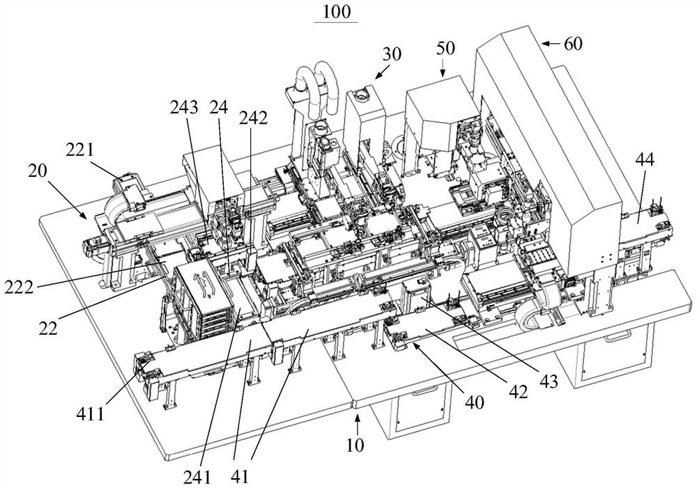
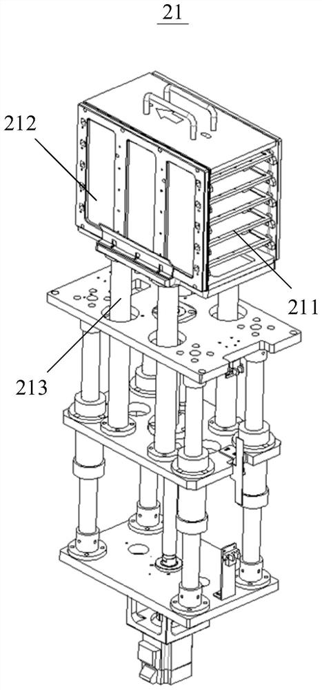
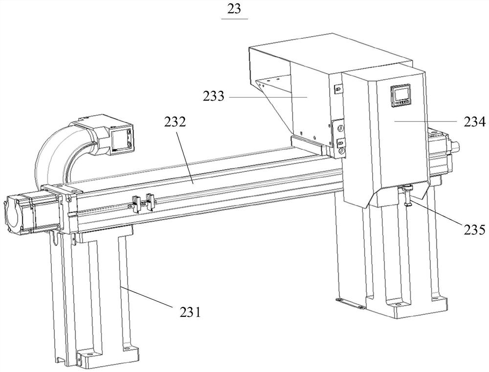
[0043] In order to facilitate understanding of the present application, the present application will be further described below with reference to the related drawings. The preferred embodiment of the present application is given. However, the present application can be implemented in many different forms, is not limited to the embodiments described herein. Conversely, the purpose of providing these embodiments is to make it more thoroughly comprehensively understood the disclosure of the present application.

[0044] The description of the following examples is illustrated with reference to the present invention, and a particular embodiment of the application can be implemented. In this paper, the serial number of the component itself, such as "first", "second", etc., only for distinguishing the described object, does not have any order or technical meaning. The "Connect", "join", including direct and indirect connections (coupled), as specifically described. The direction term me...


PUM


Abstract

The invention discloses chip laminating equipment, which is used for laminating a chip. The chip laminating equipment comprises a main worktable, and a feeding and tray placing module, a dispensing module, a carrier plate conveying module, an overturning module and an attaching module which are mounted on the main worktable, the feeding and tray placing module is used for placing a chip base at a preset feeding position, locating and detecting the chip base, and placing the located and detected chip base in a transfer tray, the dispensing module is used for locating and detecting the height of the placed chip base, performing dispensing operation on the chip base and conveying the dispensed chip base to the overturning module, the overturning module is used for overturning the chip base. The carrier plate conveying module is used for conveying a carrier plate on which a chip is mounted to the attaching module and conveying a carrier plate on which a chip base is not attached to a next attaching device, and the attaching module is used for attaching the overturned chip base to the chip of the carrier plate.

Description

Technical field [0001] The present application relates to the field of chip attachment, in particular, to a chip fitting apparatus. Background technique [0002] With the continuous improvement of science and technology, the intelligent development, the intelligent manufacturing trend is tended, and the chip manufacturing is also developed towards the direction of science and technology, intelligent and high-endization. The development of chips will inevitably require increasing chip. The higher it. At present, before the chip attachment, the chip and its carrier are needed to clean, and then manually put the cleaning carrier into the station's workbench or place the carrier to the attachment machine. Storage station, but during the carrier transfer process, it is easy to cause secondary pollution of the cleaning, and it is also required to manually pending the loop operation after transport. The uncertainty of artificial operations is easy to lead to poor product, reducing produ...

Claims


Application Information

Patent Timeline
Patent Type & Authority Applications(China)
IPC IPC(8): H01L21/677H01L21/68H01L21/66H01L21/67B05C5/02B05C13/02
CPCH01L21/67155H01L21/6715H01L21/67144H01L21/67132H01L21/67706H01L21/68H01L21/67253H01L22/10B05C5/0208B05C13/02
Inventor 陈洁陈鸣余寺强丁晓华周翔
Owner SHENZHEN EAGLE EYE ONLINE ELECTRONICS TECH
Why Eureka
Try Eureka