Scribing method of wafer with double-sided structure

A dicing and wafer technology, used in electrical components, semiconductor/solid-state device manufacturing, circuits, etc., can solve problems such as chip defects and yield reduction, and achieve the effect of improving yield and protecting structural surfaces.

Pending Publication Date: 2022-02-25
无锡微视传感科技有限公司
View PDF0 Cites 0 Cited by
  • Summary
  • Abstract
  • Description
  • Claims
  • Application Information

AI Technical Summary

Problems solved by technology

[0003] Existing paste UV film to mark the craft production method of the wafer of double-sided structure such as figure 1 As shown, first choose a double-sided structure wafer, one side is pasted on the UV film, and then the other side is diced and cut. After the cutting is completed, the UV film is cured, and finally the film is taken. The problem lies in the side pasted on the UV film. In the end, even if the UV film is cured, there are still abnormal structures that are adhered to the UV film, such as movable structures such as cantilever beams, which eventually lead to chip defects and lower yields.

Method used


Image

  • Scribing method of wafer with double-sided structure
  • Scribing method of wafer with double-sided structure
  • Scribing method of wafer with double-sided structure

Examples


Embodiment Construction

[0026] The specific embodiments of the present invention will be further described below in conjunction with the accompanying drawings.

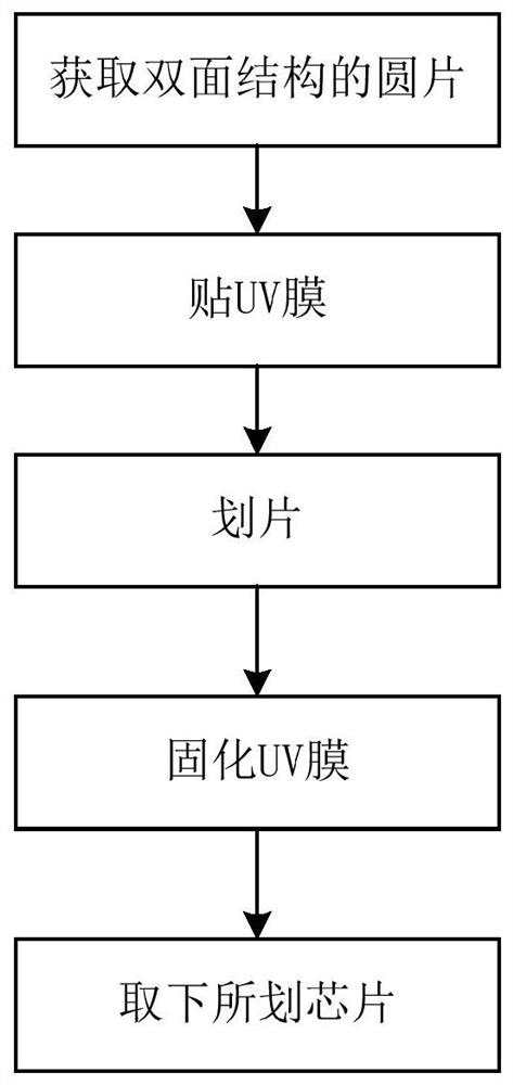
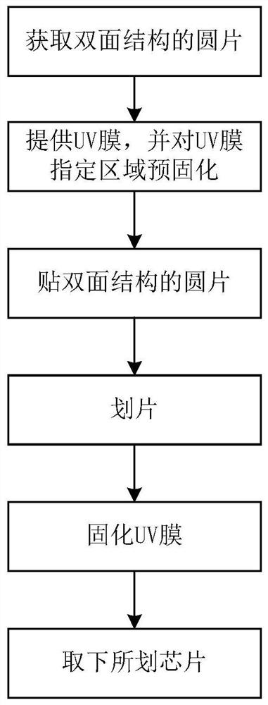
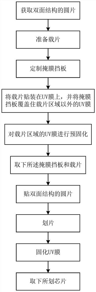
[0027] Embodiment 1 of the present invention discloses a method for dicing wafers with a double-sided structure. Please refer to figure 2 As shown in the flow chart, the scribing method of the present embodiment includes the following steps:

[0028] Obtain a wafer of double-sided structure;

[0029] Provide UV film and pre-cure the designated area of ​​the UV film;

[0030] Attach one side of the wafer to the UV film so that the pre-cured designated area completely covers the chip area on the wafer;

[0031] Scribe the wafer attached with UV film to complete the separation between the chips on the wafer;

[0032] Perform secondary curing on the UV film and remove the chip.

[0033] Preferably, the pre-curing treatment is completed by irradiation with ultraviolet lamps, and the irradiation time of ultraviolet lamps is 20s to 40s.

[00...


PUM


Abstract

The invention discloses a scribing method for a wafer with a double-sided structure, and relates to the technical field of semiconductors, and the method comprises the steps: obtaining the wafer with the double-sided structure; providing a UV film, and performing pre-curing treatment on a specified area of the UV film; enabling one side of the wafer to be attached to the UV film, so that the pre-cured designated area completely covers the chip area on the wafer; scribing the wafer attached with the UV film to complete the separation of the chips on the wafer; and carrying out secondary curing treatment on the UV film, and taking down the chip. According to the method for pre-curing the designated area of the UV film, the viscidity in the designated area of the UV film is reduced to the degree that the structural surface of the wafer cannot be damaged, and the viscidity of the UV film outside the designated area is not reduced, so while the structural surface is protected, the effect of fixing the wafer can be achieved, and after final cutting, the problem that the structure of the chip is stuck by the UV film is avoided, and the yield is improved.

Description

technical field [0001] The invention relates to the technical field of semiconductors, in particular to a method for dicing a wafer with a double-sided structure. Background technique [0002] In semiconductor processing, the use of UV film is generally common in the scribing process. It is to stick one side of the wafer on the UV film to play the role of fixing the wafer, and then cut the wafer. After the cutting is completed, the UV film is cured. , to reduce the viscosity and then remove the scribed chip. [0003] Existing paste UV film to mark the craft production method of the wafer of double-sided structure such as figure 1 As shown, first choose a double-sided structure wafer, one side is pasted on the UV film, and then the other side is diced and cut. After the cutting is completed, the UV film is cured, and finally the film is taken. The problem lies in the side pasted on the UV film. In the end, even if the UV film is cured, there are still abnormal structures th...

Claims


Application Information

Patent Timeline
Patent Type & Authority Applications(China)
IPC IPC(8): H01L21/78H01L21/67
CPCH01L21/78H01L21/67132H01L21/67115
Inventor 袁佳孙其梁徐乃涛程进
Owner 无锡微视传感科技有限公司
Why Eureka
Try Eureka