Supercharge Your Innovation With Domain-Expert AI Agents!

Method for producing thermal infrared sensor array in vacuum-filled wafer-level housing

A sensor array, wafer-level technology, applied in the direction of electric solid-state devices, semiconductor devices, instruments, etc., can solve the problems of large lateral overall size and difficult to accommodate

Pending Publication Date: 2022-02-25
HEIMANN SENSOR GMBH
View PDF4 Cites 0 Cited by
  • Summary
  • Abstract
  • Description
  • Claims
  • Application Information

AI Technical Summary

Problems solved by technology

[0035] A third disadvantage of known thermal infrared array solutions (e.g. thermopile arrays) is the large lateral overall size, which also makes it difficult to accommodate in small mobile devices such as smartphones

Method used


Image

  • Method for producing thermal infrared sensor array in vacuum-filled wafer-level housing
  • Method for producing thermal infrared sensor array in vacuum-filled wafer-level housing
  • Method for producing thermal infrared sensor array in vacuum-filled wafer-level housing

Examples


Embodiment Construction

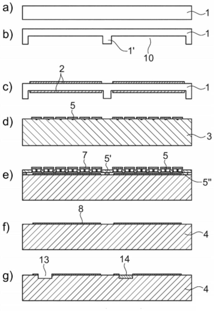
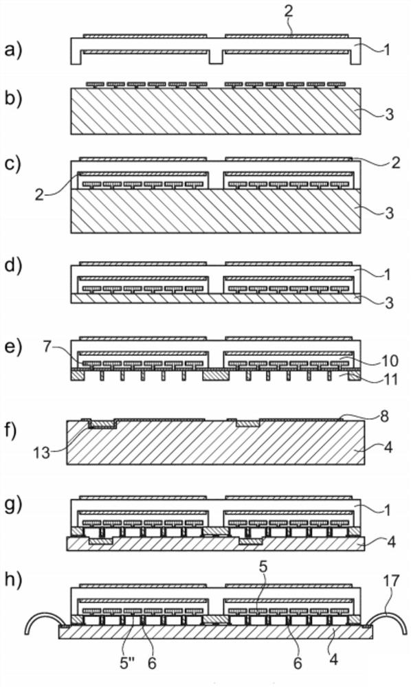
[0066] It will be appreciated that only the details of various wafers are respectively shown in Figures 1 through 9, in fact, the area of ​​these wafers is much larger, and each of which includes a plurality of as described adjacent to each other. These structures are manufactured. Single is monolithized by dividing into a separate thermal infrared sensor array.

[0067] FIG. 1 shows a basic structure of a very thin infrared sensor array in a vacuum wafer level package before the respective wafer mounting but prior to single sheet, which has an upper cover wafer 1, thinned central wafer 3 and bottom wafer 4 . In the lid wafer 1, there is a cavity 10 above a set of sensor pixels 5.

[0068] According to Figure 1, the infrared sensor array includes a plurality of groups of infrared sensor arrays having a plurality of sensor pixels 5, a narrow strip 5 ', and a cavity 10, wherein the plurality of sensor pixels 5 are adjacent to each other or four or more. The group rules are arranged,...


PUM

PropertyMeasurementUnit
thicknessaaaaaaaaaa
thicknessaaaaaaaaaa
sizeaaaaaaaaaa

Abstract

The invention relates to a method for producing a thermal infrared sensor array in a vacuum-filled wafer-level housing with particularly small dimensions. The wafer-level housing consists of at least two wafers, separately a cover wafer (1) and a central wafer (3) comprising multiple infrared-sensitive sensor pixels (5) on a respective thin slotted membrane (5'') over a heat-insulating cavity (11). The aim of the invention is to provide a method for producing a high-resolution monolithic silicon micromechanical thermopile array sensor by using a wafer level packaging technology, wherein the sensor achieves a particularly high spatial resolution capability and a very high filling degree with very small housing dimensions, in particular a very low overall thickness, and can be inexpensively produced using standard CMOS processes. This is achieved in that the cover wafer (1) is first rigidly mechanically connected to the provided central wafer (3) comprising the sensor pixels with the infrared-sensitive pixels (5) by means of wafer bonding, and the central wafer (3) is then thinned out from the wafer rear face to a specified thickness.

Description

Technical field [0001] The present invention relates to a method of producing a thermal infrared sensor array in a vacuum-filled wafer cassette in a wafer level package. Background technique [0002] For applications for small economical thermal imaging cameras, it is important that the sensor module has high spatial resolution and thermal resolution and minimum housing size. [0003] This is especially suitable for so-called mobile applications, such as smartphones, etc. [0004] These applications must achieve good measurement accuracy and high thermal resolution within the smallest space, and also have the smallest sensor module overall size. For example, in order to be able to accommodate a miniaturized thermal imaging camera constructed from the infrared array sensor module in the housing of the smartphone itself, in this case, the infrared array sensor module is particularly important. In order to be able to accommodate thermally imaging micro-camera, the total height of th...

Claims


Application Information

Patent Timeline
Patent Type & Authority Applications(China)
IPC IPC(8): H01L27/146G01J5/04G01J5/12H10N10/00H10N10/01
CPCH01L27/14618H01L27/14649H01L27/14683G01J5/045G01J5/12G01J2005/106G01J5/10G01J5/0802H01L27/14632H01L27/14687
Inventor J·希福尔戴克F·赫尔曼C·施密特W·莱纳克B·弗尔格M·西蒙M·施诺尔
Owner HEIMANN SENSOR GMBH
Features
  • R&D
  • Intellectual Property
  • Life Sciences
  • Materials
  • Tech Scout
  • Unparalleled Data Quality
  • Higher Quality Content
  • 60% Fewer Hallucinations
Learn More