
Nanoscale flexible electronic transfer printing method driven by surface tension

A surface tension, nano-level technology, applied in nanotechnology, nanotechnology, nanotechnology and other directions for materials and surface science, can solve the problems of invisible transfer process, unfavorable device precise positioning, device damage, etc. Conducive to precise positioning, large operating space, and simple overall process

Active Publication Date: 2022-03-01
DALIAN UNIV OF TECH
View PDF9 Cites 1 Cited by
  • Summary
  • Abstract
  • Description
  • Claims
  • Application Information

AI Technical Summary

Problems solved by technology

Most of the existing transfer printing methods only complete the planar transfer printing at the micron and above size level, the transfer process is invisible, which is not conducive to the precise positioning of the device, and it is necessary to apply a certain pre-pressure to control the interface adhesion strength during the transfer printing, which is may damage the device

Method used


Image

  • Nanoscale flexible electronic transfer printing method driven by surface tension
  • Nanoscale flexible electronic transfer printing method driven by surface tension
  • Nanoscale flexible electronic transfer printing method driven by surface tension

Examples


Embodiment Construction

[0030] Embodiments of the present invention will be further described below in conjunction with technical solutions and accompanying drawings.

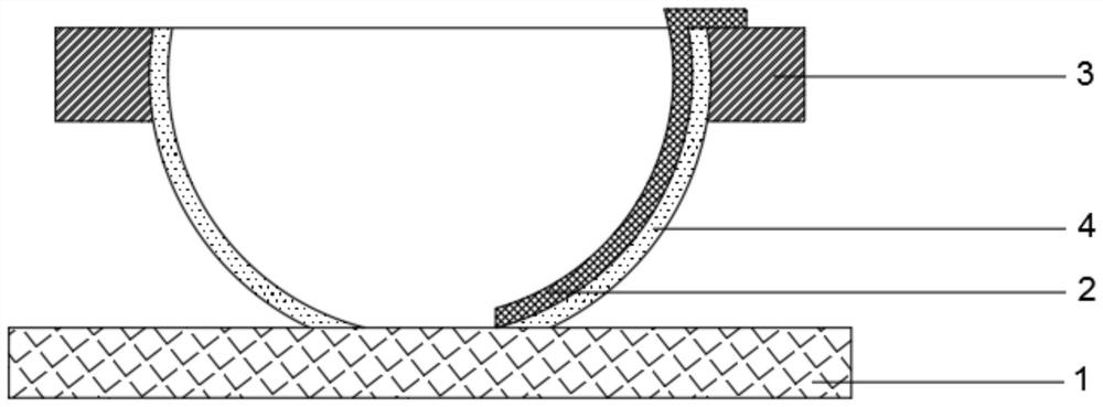
[0031] (1) if figure 1 As shown, the deionized water used to clean electronic devices (a gold film with a thickness of 600 nm with a serpentine structure) was changed to a hydrophilic liquid with viscosity and surface tension. Exemplarily, the liquid used may be, but not limited to, a sodium stearate soap solution with a concentration of 3%;

[0032] (2) if figure 2 As shown, a ring with a radius of 5 cm is placed under the electronic device film in the soap solution, a corner of the electronic device film is placed on the ring, and the ring is lifted from the soap solution at a speed of 1 cm per second. During this process, a layer of soap film will be formed between the ring that leaves the liquid surface and the soap liquid surface, and the electronic device film is attached to the soap film and gradually separates from the soap...


PUM

PropertyMeasurementUnit
thicknessaaaaaaaaaa
thicknessaaaaaaaaaa
thicknessaaaaaaaaaa

Abstract

The invention discloses a surface tension driven nanoscale flexible electronic transfer printing method. According to the method, a circular ring and viscous liquid are used for extracting and printing an electronic device film floating in cleaning liquid to any complex curved surface receptor. Due to the characteristic that a viscous liquid film is easy to break, current transfer printing does not need a traditional transfer printing interface competitive fracture and strong and weak adhesion regulation and control strategy; the liquid film does not need to introduce prestress, and is suitable for a nanoscale film which cannot bear and a receptor which does not bear pressure; the viscous liquid film is non-uniform in deformation under local load, and is suitable for non-uniform diversity and compact space curved surface transfer printing; the thickness of the viscous liquid film and the thickness of the electronic device film are in the nanometer level, and flexible electrons prepared through transfer printing can form the in-situ measurement effect; the viscous liquid film is transparent and clear, what you see is what you get, and accurate positioning of transfer printing is facilitated; the transfer printing residual viscous liquid does not cause the reduction of the electromagnetic performance of the flexible electronic device; the method is simple in process, low in requirements on electronic device films and acceptor matrix materials and good in universality.

Description

technical field [0001] The invention belongs to the technical field of micro-nano processing and flexible electronics, and relates to a nanoscale flexible electronic transfer printing method driven by surface tension. [0002] technical background [0003] Flexible electronic technology refers to the fabrication of organic or inorganic material electronic devices on flexible substrates, making flexible electronic devices stretchable and bendable, and has a wide range of applications in energy, information, medical and other fields, such as flexible Electronic displays, organic light-emitting diodes, electronic skin, etc. Transfer printing is one of the important means to realize the preparation of this technology. It is a method of transferring electronic devices from the donor (manufacturing) substrate to the acceptor (application) substrate. It mainly includes two parts of picking and placing, involving the strength of the interface. Adhesive conversion is more difficult t...

Claims


Application Information

Patent Timeline
Patent Type & Authority Applications(China)
IPC IPC(8): G09F9/30B82Y30/00
CPCG09F9/301B82Y30/00H05K3/025H05K2203/0531H05K1/028H05K2203/0766H05K3/0085H05K3/1275H05K3/4638H05K2203/14
Inventor 李明刘军山亢战车俐萱胡小光
Owner DALIAN UNIV OF TECH
Learn More