Semiconductor processing apparatus

A processing device and semiconductor technology, applied in the fields of semiconductor/solid-state device manufacturing, electrical components, circuits, etc., can solve the problems of high equipment cost and complicated methods, and achieve the effect of reducing volume

Pending Publication Date: 2022-03-15
WUXI HUAYING MICROELECTRONICS TECH CO LTD
View PDF0 Cites 0 Cited by
  • Summary
  • Abstract
  • Description
  • Claims
  • Application Information

AI Technical Summary

Problems solved by technology

The equipment cost of the plasma edge etching method is high, and the method is relatively complicated, and it is mainly used in the process of integrated circuit chips

Method used


Image

  • Semiconductor processing apparatus
  • Semiconductor processing apparatus
  • Semiconductor processing apparatus

Examples


no. 1 example

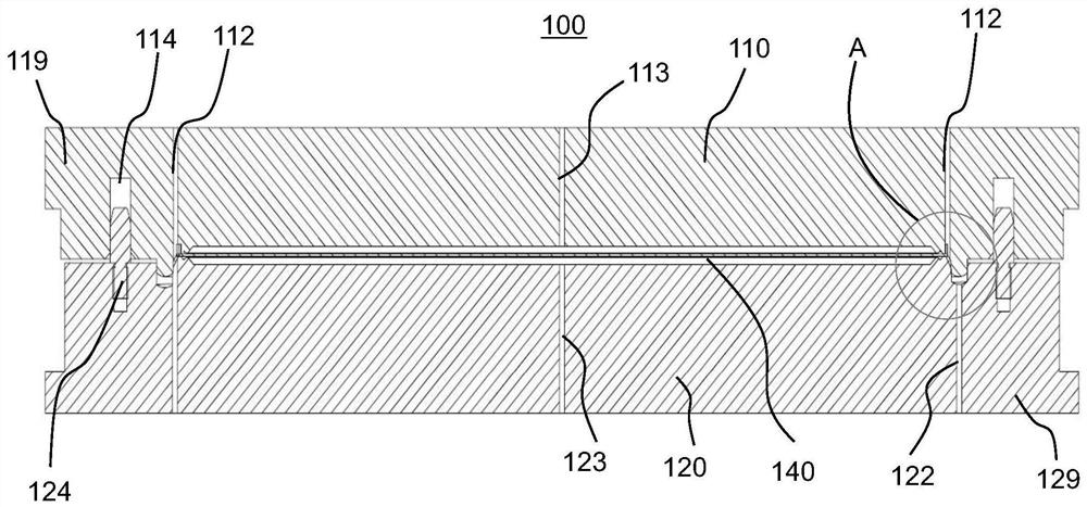
[0026] Please refer to Figure 2a to Figure 3b , which shows a schematic structural diagram of the semiconductor processing device 100 provided in the first embodiment of the present invention, wherein: Figure 2a It is a schematic cross-sectional view of the semiconductor processing device in the first embodiment of the present invention; Figure 2b for Figure 2a The enlarged schematic diagram of circle A in ; Figure 3a for Figure 2a A bottom view of the first chamber portion of the semiconductor processing apparatus in Figure 3b for Figure 2a A top view of the second chamber section of the semiconductor processing apparatus in .

[0027] Please refer to Figure 2a to Figure 3b , the semiconductor processing apparatus 100 includes a first chamber part 110 and a second chamber part 120 . The first chamber portion 110 includes a first chamber plate 119 and a flange 118 extending from a periphery of the first chamber plate 119 . The second chamber portion 120 includ...

no. 2 example

[0047] Please refer to Figure 4 to Figure 6b , which shows a schematic structural diagram of the semiconductor processing device 200 provided in the second embodiment of the present invention, wherein: Figure 4 It is a schematic cross-sectional view of the semiconductor processing device in the first embodiment of the present invention; Figure 5 for Figure 4 The enlarged schematic diagram of circle B in ; Figure 6a for Figure 4 A bottom view of the first chamber portion of the semiconductor processing apparatus in Figure 6b for Figure 4 A top view of the second chamber section of the semiconductor processing apparatus in .

[0048] The structure of the semiconductor processing device 200 in the second embodiment is mostly the same as that of the semiconductor processing device 100 in the first embodiment, so the same parts are marked with the same marks, and the difference between the two is mainly: semiconductor processing There are some differences in the struc...


PUM


Abstract

The invention provides a semiconductor processing apparatus. The semiconductor processing apparatus comprises a first chamber part; and a second chamber part. The first cavity part is provided with a first channel, the second cavity part is provided with a second channel, and when the second cavity part is located at a closed position relative to the first cavity part and a semiconductor wafer is accommodated in the microcavity, the first channel and the second channel are communicated and jointly form an edge microprocessing space at the edge of the wafer; the outer edge of the semiconductor wafer accommodated in the microchamber extends into the edge microprocessing space. The first cavity part is provided with a sealing joint part located on the outer side of the first channel, the second cavity part is provided with a joint groove corresponding to the sealing joint part, and by means of the edge micro-processing space, processing of the outer edge of the semiconductor wafer can be achieved.

Description

【Technical field】 [0001] The invention relates to the field of surface treatment of semiconductor wafers or similar workpieces, in particular to semiconductor processing devices. 【Background technique】 [0002] The precise edge etch process of semiconductor wafers is a challenging process. It requires micron-scale precise etching of the wafer edge without damaging or contaminating the remaining film. In the epitaxial wafer manufacturing process and advanced integrated circuit manufacturing process, the wafer edge etching process is an important step to ensure the quality of film formation and improve chip yield. [0003] Please refer to Figure 1a to Figure 1d ,in: Figure 1a A schematic structural view of a semiconductor wafer 400 is shown, Figure 1b for Figure 1a The E-E sectional view of; Figure 1c a partial cross-sectional view of an outer edge of a semiconductor wafer prior to edge processing; Figure 1d is a cross-sectional view of the outer edge portion of th...

Claims


Application Information

Patent Timeline
IPC IPC(8): H01L21/687H01L21/67
CPCH01L21/67075H01L21/68785H01L21/68735H01L21/6708H01L21/67092
Inventor 温子瑛
Owner WUXI HUAYING MICROELECTRONICS TECH CO LTD
Why Eureka
Try Eureka