

Anode back plate for 3D printing
A 3D printing and anode technology, applied in the field of 3D printing, can solve the problems of inability to improve the aspect ratio of the driving transistor and the destruction of the active layer of the transistor, and achieve the effect of large aspect ratio, preventing damage and improving the driving ability.
- Summary
- Abstract
- Description
- Claims
- Application Information
AI Technical Summary
Problems solved by technology
Method used
Image

Examples
Embodiment approach
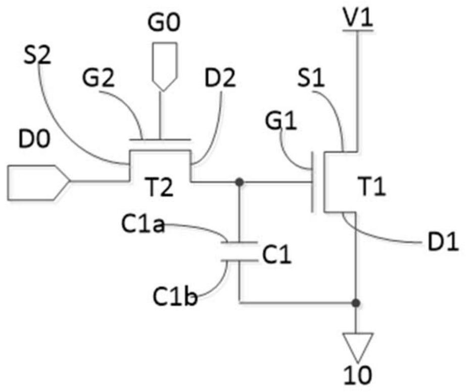
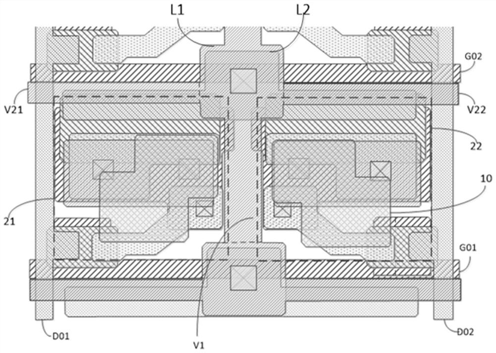
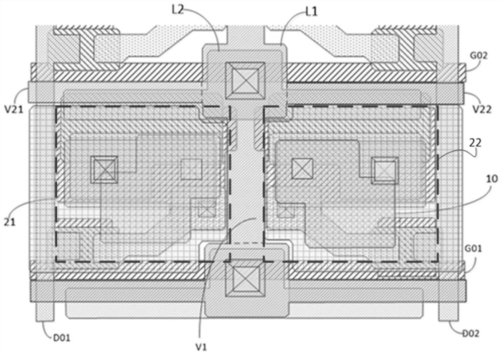
[0091] According to another specific implementation manner, the conductive patterns included in the conductive layer may be continuous with each other, and the orthographic projection of the conductive pattern on the base substrate covers the orthographic projection of the active layer pattern on the base substrate.
[0092] Such as figure 2 and Figure 4 As shown, the first gate line G01 has a first protrusion, the main body of the first gate line G01 extends along the row direction, the first protrusion protrudes from the main body of G01, and the gate G2 of the switching transistor is the first protrusion, so that the space occupied by the switching transistor is small;
[0093] Such as figure 2 and Figure 7 As shown, the first data line D01 has a second protrusion, the main body of the first data line D01 extends along the column direction, the second protrusion protrudes from the main body of D01, and the source S2 of the switching transistor is The second protrudi...
PUM
 Abstract
Description
Claims
Application Information