Semiconductor memory device
A semiconductor and memory technology, applied in the field of three-dimensional semiconductor memory devices, can solve the problems of increased integration density and limitations of two-dimensional semiconductor devices
- Summary
- Abstract
- Description
- Claims
- Application Information
AI Technical Summary
Problems solved by technology
Method used
Image


Examples
Embodiment Construction
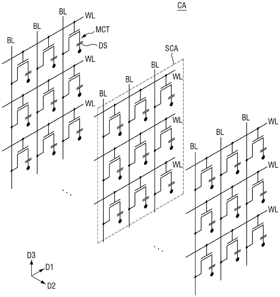
[0025] figure 1 is a simplified circuit diagram illustrating a cell array of a three-dimensional (3D) semiconductor memory device according to at least one example embodiment.
[0026] refer to figure 1 , the cell array CA of the 3D semiconductor memory device according to at least one example embodiment may include a plurality of sub-cell arrays SCA, but example embodiments are not limited thereto. The sub-cell array SCA may be arranged along the second direction D2 of the cell array CA, but is not limited thereto. According to some example embodiments, a 3D semiconductor memory device may include a plurality of cell arrays CA, but example embodiments are not limited thereto.
[0027] Each of the sub-cell arrays SCA may include a plurality of bit lines BL, a plurality of word lines WL, and / or a plurality of memory cell transistors MCT, and the like. One memory cell transistor MCT may be included between one word line WL and one bit line BL (for example, arranged between on...
PUM
 Abstract
Description
Claims
Application Information
 - R&D
- Intellectual Property
- Life Sciences
- Materials
- Tech Scout
- Unparalleled Data Quality
- Higher Quality Content
- 60% Fewer Hallucinations
Browse by: Latest US Patents, China's latest patents, Technical Efficacy Thesaurus, Application Domain, Technology Topic, Popular Technical Reports.
© 2025 PatSnap. All rights reserved.Legal|Privacy policy|Modern Slavery Act Transparency Statement|Sitemap|About US| Contact US: help@patsnap.com