
Chip mounting equipment for integrated circuit processing

A technology of integrated circuit and patch, applied in the direction of electrical components, electrical components, etc., can solve the problems of residual residue, insufficient amount of solder paste on the circuit board, and inability to replenish the amount of solder paste, etc., and achieve the effect of improving the efficiency of placement

Inactive Publication Date: 2022-04-01
深圳市世纪众云科技有限公司
View PDF0 Cites 0 Cited by
  • Summary
  • Abstract
  • Description
  • Claims
  • Application Information

AI Technical Summary

Problems solved by technology

[0003] When the traditional integrated circuit is being processed, a steel plate with holes is often placed on the circuit board. The holes on the steel plate correspond to the positions on the circuit board that need to be patched. Apply solder paste on one side of the steel plate. The push plate spreads the solder paste evenly on the steel plate, so that the solder paste enters the hole groove and spreads on the circuit board, and then attaches the chip device to the circuit board through the placement machine, and liquefies the solder paste by baking. Solidification, so that the patch device is fixedly attached to the steel plate; but this processing method has the following problems: the position of the steel plate is fixed before the operation, and the circuit board moves upward relative to the steel plate until the steel plates touch each other. Under the action of the push plate, The solder paste enters the hole slot and adheres to the top of the circuit board. Due to the properties of the solder paste itself, it will leave residue on the steel plate, resulting in insufficient solder paste on the circuit board, which will affect the stability of the subsequent placement. Moreover, the existing SPI inspection can only detect whether the amount of solder paste on the circuit board meets the requirements of placement, but cannot supplement the amount of solder paste

Method used


Image

  • Chip mounting equipment for integrated circuit processing
  • Chip mounting equipment for integrated circuit processing
  • Chip mounting equipment for integrated circuit processing

Examples


Embodiment Construction

[0033] The following will clearly and completely describe the technical solutions in the embodiments of the present invention with reference to the accompanying drawings in the embodiments of the present invention. Obviously, the described embodiments are only some, not all, embodiments of the present invention. Based on the embodiments of the present invention, all other embodiments obtained by persons of ordinary skill in the art without making creative efforts belong to the protection scope of the present invention.

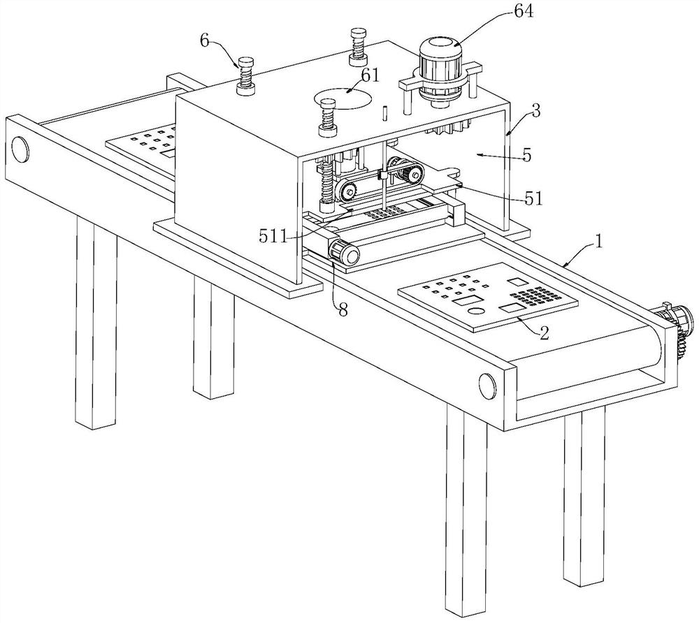
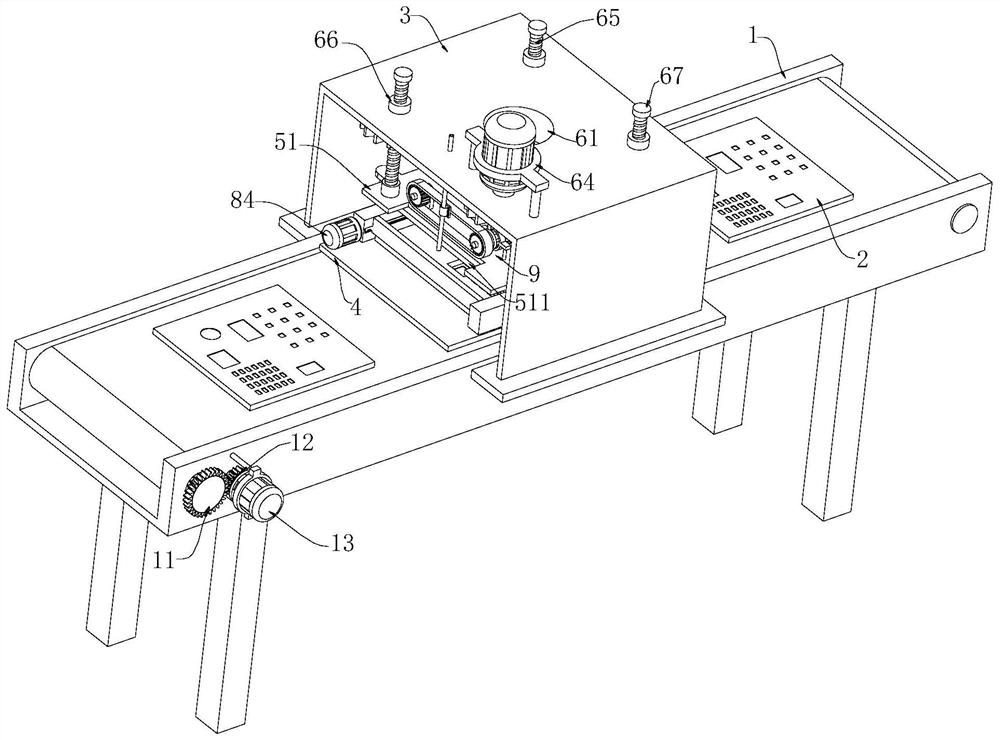
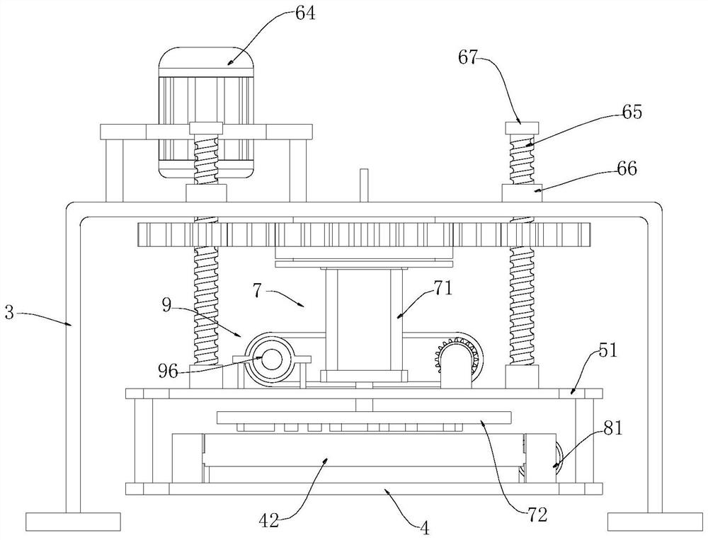
[0034] see Figure 1-10 , the present invention provides a technical solution: a chip placement device for integrated circuit processing, including a transmission belt 1, a plurality of circuit boards 2 are equidistantly placed on the transmission belt 1, a fixing frame 3 is arranged above the transmission belt 1, and the fixing frame 3- There is a patch frame on the side, which is not shown in the figure. After the solder paste is applied, the transmission be...


PUM


Abstract

The invention discloses chip mounting equipment for integrated circuit processing, which comprises a transmission belt, a circuit board is arranged on the transmission belt, a fixing frame is arranged above the transmission belt, a steel plate with a hole groove is arranged below the fixing frame and at a position right opposite to the circuit board, and a lifting part for driving the steel plate to lift relative to the circuit board is arranged between the fixing frame and the steel plate. The lifting part comprises a moving plate and an adjusting part, a reserved space is formed between the moving plate and the steel plate, a material pressing part is arranged in the reserved space, a push plate is arranged on one side of the steel plate, material pushing parts for driving the push plate to push solder paste are arranged on the two sides of the steel plate, and a coating part for evenly coating the solder paste is arranged above the push plate. According to the chip mounting equipment for integrated circuit processing, after the hole groove in the steel plate is limited and coated with solder paste through the stop block on the stop plate, the stop block descends to the position over the hole groove, the stop block plays a role in pressing the solder paste in the hole groove, and therefore the solder paste is left on the surface of a circuit board and prevented from being excessively attached to the steel plate.

Description

technical field [0001] The invention relates to the technical field of integrated circuit processing, in particular to a patching device for integrated circuit processing. Background technique [0002] An integrated circuit is a way to miniaturize a circuit (mainly including semiconductor equipment, including passive components, etc.). It adopts a certain process to interconnect the transistors, resistors, capacitors, inductors and other components and wiring required in a circuit. One or several small semiconductor wafers or dielectric substrates, and then packaged in a package to become a microstructure with the required circuit functions; all the components have been structurally integrated to make electronic components miniaturized , low power consumption, intelligence and high reliability have taken a big step forward. In the environment of rapid development of science and technology, electrical appliances have played an irreplaceable role in people's daily life, wheth...

Claims


Application Information

Patent Timeline
Patent Type & Authority Applications(China)
IPC IPC(8): H05K13/00H05K13/04
Inventor 王倍昌于明明
Owner 深圳市世纪众云科技有限公司
Learn More