Transfer method of light-emitting chip, display panel and display device

A light-emitting chip and transfer method technology, which is applied in the direction of electrical components, electric solid devices, circuits, etc., can solve the problems of elastic mold grasping and Micro light-emitting chips being inconvenient, and achieve the goal of increasing the transfer yield and improving the transfer yield Effect

Pending Publication Date: 2022-04-05
CHONGQING KONKA PHOTOELECTRIC TECH RES INST CO LTD
View PDF0 Cites 2 Cited by
  • Summary
  • Abstract
  • Description
  • Claims
  • Application Information

AI Technical Summary

Problems solved by technology

[0004] In view of the above deficiencies in the prior art, the purpose of the present application is to provide a method for transferring light-emitting chips, a display panel and a display dev

Method used


Image

  • Transfer method of light-emitting chip, display panel and display device
  • Transfer method of light-emitting chip, display panel and display device
  • Transfer method of light-emitting chip, display panel and display device

Examples


Embodiment Construction

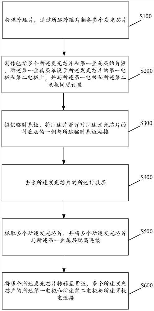
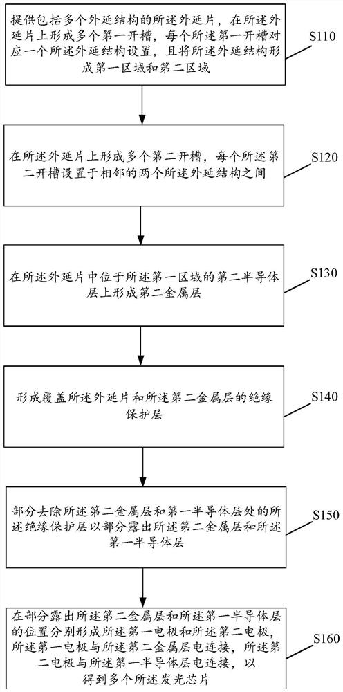
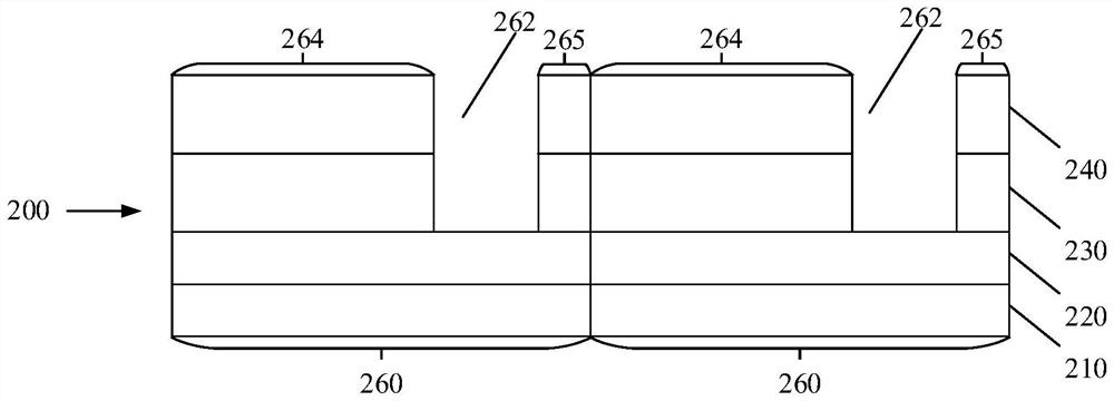
[0062] In order to facilitate the understanding of the present application, the present application will be described more fully below with reference to the relevant drawings. Preferred embodiments of the application are shown in the accompanying drawings. However, the present application can be embodied in many different forms and is not limited to the embodiments described herein. On the contrary, the purpose of providing these embodiments is to make the disclosure of the application more thorough and comprehensive.

[0063] Unless otherwise defined, all technical and scientific terms used herein have the same meaning as commonly understood by one of ordinary skill in the technical field to which this application belongs. The terminology used herein in the description of the application is only for the purpose of describing specific implementations, and is not intended to limit the application.

[0064] With the maturity of manufacturing process and the drop of price, ther...


PUM

PropertyMeasurementUnit
Thicknessaaaaaaaaaa
Thicknessaaaaaaaaaa

Abstract

The invention relates to a light-emitting chip transfer method, and the method comprises the steps: providing an epitaxial wafer, and preparing a plurality of light-emitting chips through the epitaxial wafer; a film source comprising the multiple light-emitting chips and a first metal layer is manufactured, the first metal layer covers the first electrodes and the second electrodes of the light-emitting chips, and the first metal layer, the first electrodes and the second electrodes are arranged at intervals; providing a temporary substrate, and bonding one side, back to the substrate layer of the light-emitting chip, of the film source with the temporary substrate; removing the substrate layer of the light-emitting chip; the plurality of light-emitting chips are grabbed, and the plurality of light-emitting chips are separated from the first metal layer; and the multiple light-emitting chips are transferred to a back plate, the first electrodes and the second electrodes of the multiple light-emitting chips are electrically connected with the back plate, and the problem that in the prior art, the light-emitting chips cannot be conveniently grabbed is solved. The invention further provides a display panel and a display device with the display panel.

Description

technical field [0001] The present application relates to the field of display technology, in particular to a method for transferring a light-emitting chip, a display panel, and a display device with the display panel. Background technique [0002] Micro Light Emitting Diode (Micro LED) is a new generation of display technology. Compared with traditional LEDs, it has high resolution, low power consumption, high brightness, high contrast, high color saturation, fast response, Thin thickness, long life and other characteristics. With the maturity of the manufacturing process and the decline of prices, there have been more and more related display products based on light-emitting chips such as Micro LEDs in recent years, such as TVs and mobile phone screens. Since display products have a low tolerance for pixel errors, improving the yield of transferred light-emitting chips is particularly important for improving the yield of display products. [0003] At present, commonly us...

Claims


Application Information

Patent Timeline
IPC IPC(8): H01L27/15H01L33/00H01L33/62
Inventor 戴广超马非凡曹进赵世雄王子川
Owner CHONGQING KONKA PHOTOELECTRIC TECH RES INST CO LTD
Why Eureka
Try Eureka