
Semiconductor package device and manufacturing method thereof

A packaging device and semiconductor technology, applied in semiconductor/solid-state device manufacturing, semiconductor devices, electric solid-state devices, etc., can solve the problems of small spacing between Nanowires, inability to fully bond, Nanowires cannot be combined with Pad, etc., to avoid voids, not easy The effect of the bridging phenomenon

Pending Publication Date: 2022-04-12
ADVANCED SEMICON ENG INC
View PDF0 Cites 0 Cited by
  • Summary
  • Abstract
  • Description
  • Claims
  • Application Information

AI Technical Summary

Problems solved by technology

[0004] (1) When bonding, the pitch between the Nanowires is small, which may not allow the underfill to flow through and cause voids (Void)
[0005] (2) When the Nanowire is directly bonded to the pad on the opposite side, it may not be fully bonded due to the Coplanarity problem of the Nanowire, that is, part of the Nanowire cannot be combined with the Pad

Method used


Image

  • Semiconductor package device and manufacturing method thereof
  • Semiconductor package device and manufacturing method thereof
  • Semiconductor package device and manufacturing method thereof

Examples


Embodiment Construction

[0029] The specific implementation manners of the present disclosure will be described below in conjunction with the accompanying drawings and examples. Those skilled in the art can easily understand the technical problems solved by the present disclosure and the technical effects produced through the contents recorded in this specification. It should be understood that the specific embodiments described here are only used to explain related inventions, rather than to limit the invention. In addition, for the convenience of description, only the parts related to the related invention are shown in the drawings.

[0030] It should be readily understood that the meanings of "on", "over" and "over" in this disclosure should be interpreted in the broadest possible manner such that "on" Not only does it mean "directly on something", but it also means "on something" including an intermediate component or layer that exists between the two.

[0031] In addition, for the convenience of...


PUM

PropertyMeasurementUnit
melting pointaaaaaaaaaa

Abstract

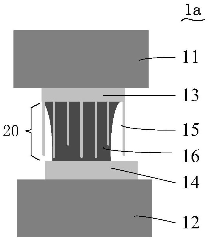
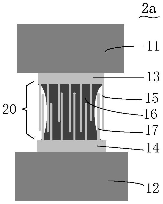
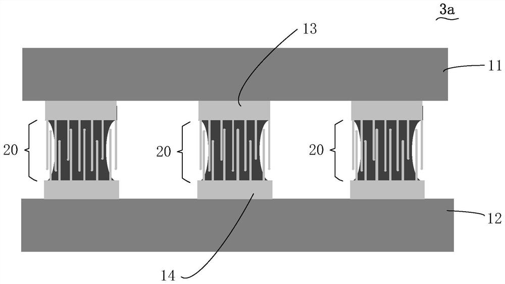
According to the semiconductor packaging device and the manufacturing method thereof, a plurality of nanowires are extended on a conductive pad, and a liquid conductive material is added between the nanowires for bonding, so that a conductive interconnection body located in a nanowire coating range is formed, and the problems existing in nanowire bonding are solved. The liquid conductive material forms a conductive interconnection body to fill gaps among the nanowires, so that the problem of cavities can be effectively avoided; the conductive interconnection body plays a role in electric connection, and the problem that the nanowire on one side cannot be completely combined with the conductive pad on the opposite side can be avoided; the liquid conductive material forms a conductive interconnection body which is located within the coating range of the nanowire, and the bridging phenomenon is not prone to being caused.

Description

technical field [0001] The present disclosure relates to the technical field of semiconductor packaging, in particular to a semiconductor packaging device and a manufacturing method thereof. Background technique [0002] In the field of semiconductor packaging, as the manufacturing process continues to shrink, traditional solder (Solder) encounters many problems. Compared with the traditional Solder, the copper (Cu)-Cu docking method has the advantages of being conducive to shrinkage and good electrical properties, but the higher bonding temperature and pressure and high cost are the problems faced by this technology. Fabricating nanowires (Nanowire) on the conductive pad (Pad) as a joint can effectively reduce the joint temperature. [0003] However, Nanowire bonding also faces some problems, including: [0004] (1) When bonding, the pitch between the Nanowires is small, which may not allow the underfill to flow through, resulting in voids. [0005] (2) When the Nanowire...

Claims


Application Information

Patent Timeline
Patent Type & Authority Applications(China)
IPC IPC(8): H01L21/60B82Y30/00
CPCH01L2224/13078H01L2224/81193
Inventor 江照泽方绪南
Owner ADVANCED SEMICON ENG INC
Learn More