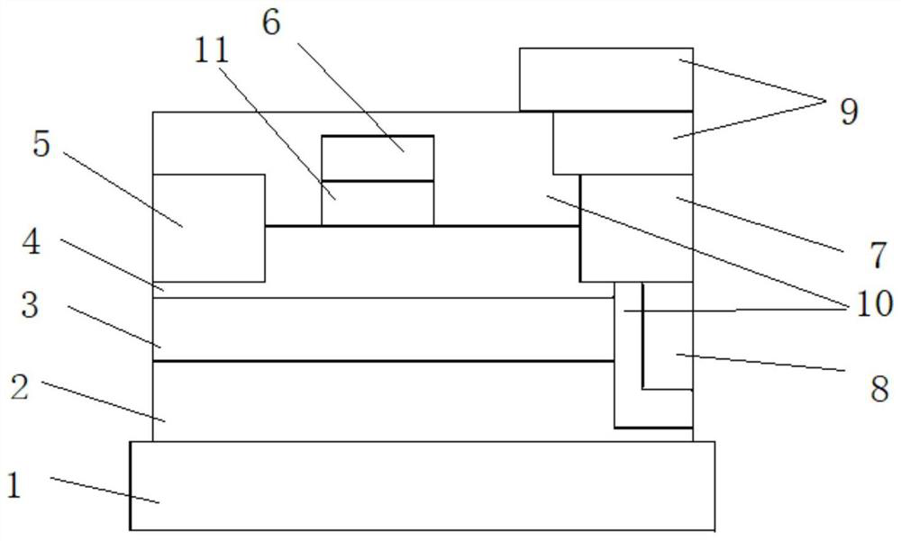
Semiconductor device

A semiconductor and device technology, applied in the field of semiconductor devices, can solve the problems of device failure, prominent limitations of the drain lateral field plate, and aggravated impact ionization in the gate region, achieve high breakdown electric field characteristics, and improve off-state breakdown. The effect of voltage

Pending Publication Date: 2022-04-12
XIAN JIAOTONG LIVERPOOL UNIV
View PDF3 Cites 0 Cited by
  • Summary
  • Abstract
  • Description
  • Claims
  • Application Information

AI Technical Summary

Problems solved by technology

[0002] With the commercial popularization of P-type GaN devices, GaN devices used in 5G radio frequency communications require smaller lateral dimensions, but with the reduction of lateral dimensions, the limitations of the lateral field plate of the drain are becoming more and more limited. protrude
This is because in the shorter gate-drain region, the slightly longer drain field plate will intensify the impact ionization phenomenon in the gate region, so the device failure problem caused by high electric field will appear in the gate edge region

Method used


Image

  • Semiconductor device

Examples


Embodiment Construction

[0016] It should be noted that, in the case of no conflict, the embodiments in the present application and the features in the embodiments can be combined with each other.

[0017] In the description of the present application, it should be understood that the terms "center", "longitudinal", "transverse", "upper", "lower", "front", "rear", "left", "right", " The orientation or positional relationship indicated by "vertical", "horizontal", "top", "bottom", "inner", "outer", etc. is based on the orientation or positional relationship shown in the drawings, and is only for the convenience of describing the present application and Simplified descriptions do not indicate or imply that the device or element referred to must have a specific orientation, be constructed and operate in a specific orientation, and thus should not be construed as limiting the scope of protection of the present application. In addition, the terms "first", "second", etc. are used for descriptive purposes on...


PUM

PropertyMeasurementUnit
Thicknessaaaaaaaaaa

Abstract

A semiconductor device comprises a substrate, a buffer layer, a channel layer, a barrier layer, a source electrode, a grid electrode, a drain electrode, a longitudinal field plate and a transverse field plate, the buffer layer, the channel layer and the barrier layer are sequentially stacked and formed above the substrate, and the source electrode, the grid electrode and the drain electrode are formed above the barrier layer at intervals. The longitudinal field plate is formed below the drain electrode and penetrates through at least part of the buffer layer, the channel layer and the barrier layer, and the transverse field plate is formed above the drain electrode and at least part of the transverse field plate is located between the drain electrode and the grid electrode. According to the semiconductor device, the high breakdown electric field characteristic is achieved by arranging the field plates of the transverse field plate and the longitudinal field plate; the longitudinal field plate and the transverse field plate play a role in dispersing electric field peaks, the longitudinal field plate below the drain electrode can effectively disperse a high electric field, and the off-state breakdown voltage of the device can be greatly improved by combining the drain electrode horizontal step field plate technology.

Description

【Technical field】 [0001] The invention relates to the technical field of semiconductor manufacturing, in particular to a semiconductor device. 【Background technique】 [0002] With the commercial popularization of P-type GaN devices, GaN devices used in 5G radio frequency communication require smaller lateral dimensions, but with the reduction of lateral dimensions, the limitations of the lateral field plate of the drain are becoming more and more limited. protrude. This is because in the shorter gate-drain region, the slightly longer drain field plate will intensify the impact ionization phenomenon in the gate region, so the device failure problem caused by high electric field will appear in the gate edge region. 【Content of invention】 [0003] An object of the present invention is to provide a semiconductor device having a high breakdown voltage. [0004] The purpose of the present invention is to realize through the following technical solutions: [0005] A semiconduc...

Claims


Application Information

Patent Timeline
IPC IPC(8): H01L29/06H01L29/20H01L29/40H01L29/78
Inventor 梁烨刘雯
Owner XIAN JIAOTONG LIVERPOOL UNIV
Why Eureka
Try Eureka