High-reliability N-type transverse insulated gate bipolar device and preparation process thereof

A bipolar device and preparation process technology, applied in semiconductor/solid-state device manufacturing, semiconductor devices, electrical components, etc., can solve the problems of unsatisfactory device reliability, significant impact ionization rate, high electric field intensity, etc. The effect of reducing the longitudinal electric field strength, increasing the off-state breakdown voltage, and increasing the on-state breakdown voltage

Active Publication Date: 2015-07-01
SOUTHEAST UNIV
View PDF3 Cites 0 Cited by
  • Summary
  • Abstract
  • Description
  • Claims
  • Application Information

AI Technical Summary

Problems solved by technology

In this case, the electric field lines under the beak of the device are dense, the electric field intensity is high, the impact ionization rate is significant, and the reliability of the device is not satisfactory.

Method used


Image

  • High-reliability N-type transverse insulated gate bipolar device and preparation process thereof
  • High-reliability N-type transverse insulated gate bipolar device and preparation process thereof
  • High-reliability N-type transverse insulated gate bipolar device and preparation process thereof

Examples


Embodiment Construction

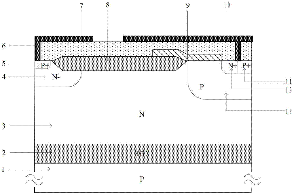
[0064] Attached below figure 2 , the present invention is described in detail, a high reliability N-type lateral insulated gate bipolar device, comprising: a P-type substrate 1, a buried oxygen 2 is arranged on the P-type substrate 1, and a buried oxygen 2 is arranged on the buried oxygen 2 There is an N-type well 3, an N-type buffer well 4 and a P-type body region 13 are arranged inside the N-type well 3, a P-type anode region 5 is arranged in the N-type buffer well 4, and a P-type body region 13 is provided with There is an N-type cathode region 12 and a P-type body contact region 11, a field oxide layer 8 is provided on the surface of the N-type well 3 and one end of the field oxide layer 8 extends to the P-type anode region 5 and ends at the P-type anode region 5, The other end extends to the P-type body region 13 and ends at the front end of the P-type body region 13. On the surface of the P-type body region 13, a polysilicon gate 9 is provided and the polysilicon gate 9...


PUM


Abstract

The invention relates to a high-reliability N-type transverse insulated gate bipolar device and a preparation process thereof. The high-reliability N-type transverse insulated gate bipolar device comprises a P-type substrate. Buried oxides are arranged on the P-type substrate. An N-type well is arranged on the buried oxides. An N-type buffer well and a P-type body region are arranged in the N-type well. A P-type anode region is arranged in the N-type buffer well. An N-type cathode region and a P-type body contact region are arranged in the P-type body region. A field oxidation layer is arranged on the surface of the N-type well. A polycrystalline silicon gate is arranged on the surface of the P-type body region. Passivation layers are respectively arranged on the surfaces of the field oxidation layer, the P-type body contact region, the N-type cathode region, the polycrystalline silicon gate and the P-type anode region. The high-reliability N-type transverse insulated gate bipolar device is characterized in that the thickness of the field oxidation layer which is embedded in the N-type well accounts for 60-80 percent of total thickness and the ratio of the thickness of the part exposed out of the N-type well of the field oxidation layer to the thickness of the part embedded in the N-type well of the field oxidation layer is enabled to be 2:3 to 1:4. Therefore, the electric field intensity and the impact ionization rate at the bird's beak of the device are obviously weakened and the reliability of the device is greatly improved.

Description

technical field [0001] The invention mainly relates to the field of high-voltage power semiconductor devices, specifically, an N-type transverse insulated gate bipolar device with high reliability and its preparation process, which is suitable for plasma flat panel display equipment, half-bridge drive circuits and automobile production field and other driver chips. Background technique [0002] With the rapid development of high-voltage integrated circuits and the continuous improvement of process technology, the lateral insulated gate bipolar transistor (Lateral Insulated Gate Bipolar Transistor, LIGBT) came out under this situation. Its unique working mechanism, namely The working mechanism of MOS devices combined with bipolar devices greatly reduces the on-resistance and greatly improves the performance of devices and circuits. Because LIGBT devices work in a high-voltage, high-current environment, they face very severe reliability problems. The end of the channel regio...

Claims


Application Information

Patent Timeline
IPC IPC(8): H01L29/739H01L21/331H01L21/762
Inventor 刘斯扬于朝辉于冰张春伟孙伟锋陆生礼时龙兴
Owner SOUTHEAST UNIV
Why Eureka
Try Eureka