LDMOS device and forming method thereof

A technology of devices and doped regions, which is applied in the direction of semiconductor devices, semiconductor/solid-state device manufacturing, electrical components, etc., to achieve the effect of improving the off-state breakdown voltage

Active Publication Date: 2021-12-31
SHANGHAI HUAHONG GRACE SEMICON MFG CORP
View PDF9 Cites 0 Cited by
  • Summary
  • Abstract
  • Description
  • Claims
  • Application Information

AI Technical Summary

Problems solved by technology

The off-state breakdown voltage and on-state breakdown voltage have a great relationship with the doping concentration of the drift region of the device, however, due to the different positions of the strongest point of impact ionization in the on-state breakdown and off-state breakdown states of the device , the existing means are difficult to meet the needs of increasing the breakdown voltage of the off-state and the breakdown voltage of the on-state at the same time
[0004] The semiconductor structure formed by the existing LDMOS device technology needs to be further improved

Method used


Image

  • LDMOS device and forming method thereof
  • LDMOS device and forming method thereof
  • LDMOS device and forming method thereof

Examples


Embodiment Construction

[0023] As mentioned in the background, the performance of devices formed by using the existing LDMOS technology needs to be improved urgently. Now combine a kind of LDMOS device to explain and analyze.

[0024] It should be noted that the "surface" and "upper" in this specification are used to describe the relative positional relationship in space, and are not limited to direct contact.

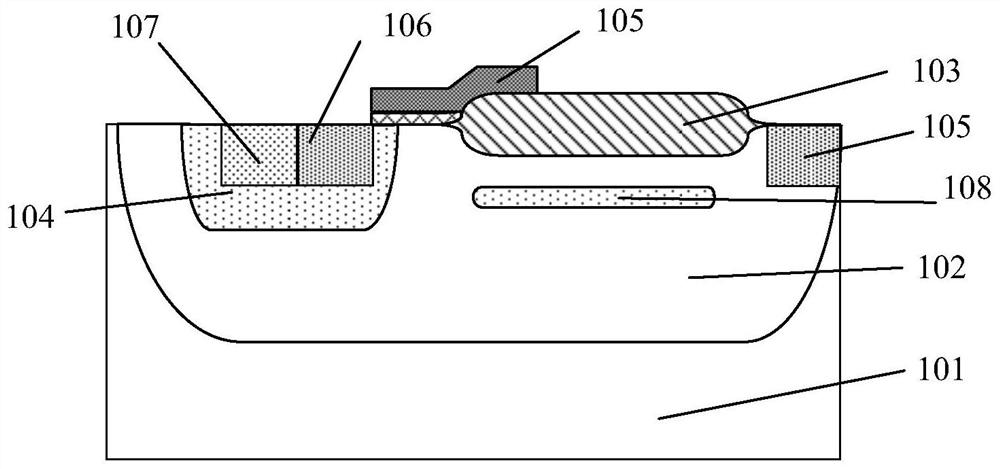
[0025] figure 1 It is a schematic diagram of a cross-sectional structure of an LDMOS device.

[0026] Please refer to figure 1, a schematic cross-sectional structure of an LDMOS device, comprising: a substrate 101; a deep well region 102 located in the substrate 101, the deep well region 102 having a first conductivity type; a surface located on the surface of the deep well region 102 The field oxygen layer 103; the body region 104 in the deep well region 102 on one side of the field oxygen layer 103, the body region 104 has a second conductivity type; the deep well region on the other sid...


PUM


Abstract

The invention discloses an LDMOS device and a forming method thereof. The method comprises the following steps: forming a field oxide layer on the surface of a deep well region, wherein the field oxide layer comprises a field oxide region and a beak region located at one end of the field oxide region in a first direction, the beak region is located on the surface of a first diffusion region, a part of the field oxide region is located on the surface of a second diffusion region, the field oxide layer has a third size in the first direction, the proportion range of the first distance to the third size is smaller than or equal to 30%, and the proportion range of the second distance to the third size is 20-80%; after the field oxide layer is formed, forming a body region is formed in the first doped region, wherein the body region has a first conductive type; and forming a grid electrode on the surface of a part of the field oxide layer, and enabling the grid electrode to further extend to the surface of a part of the body region. Different target breakdown voltage performance can be achieved by selecting different first distances and second distances.

Description

technical field [0001] The invention relates to the technical field of semiconductor manufacturing, in particular to an LDMOS device and a forming method thereof. Background technique [0002] LDMOS devices (Lateral Double-Diffused Metal Oxide Semiconductor Field Effect Transistor, Lateral Double-Diffused Metal Oxide Semiconductor Field Effect Transistor) in high-voltage power devices have good process compatibility with CMOS devices due to the characteristics of current flowing laterally on the device surface. At the same time, compared with traditional power devices, LDMOS devices are widely used because of their good characteristics of high breakdown voltage and low on-resistance. [0003] In LDMOS devices, off-state breakdown voltage (Off-BV) and on-state breakdown voltage (On-BV) are important indicators. The off-state breakdown voltage and on-state breakdown voltage have a great relationship with the doping concentration of the drift region of the device, however, due...

Claims


Application Information

Patent Timeline
Patent Type & Authority Applications(China)
IPC IPC(8): H01L29/06H01L29/78H01L21/336
CPCH01L29/0615H01L29/7816H01L29/66681
Inventor 段文婷钱文生
Owner SHANGHAI HUAHONG GRACE SEMICON MFG CORP
Why Eureka
Try Eureka