ldmos device and its manufacturing method

A manufacturing method and device technology, applied in semiconductor/solid-state device manufacturing, semiconductor devices, electrical components, etc., capable of solving problems such as Rsp increase

Active Publication Date: 2020-06-09
SHANGHAI HUAHONG GRACE SEMICON MFG CORP
View PDF5 Cites 0 Cited by
  • Summary
  • Abstract
  • Description
  • Claims
  • Application Information

AI Technical Summary

Problems solved by technology

However, enlarging the lateral dimension will cause the Rsp of the device to increase rapidly

Method used


Image

  • ldmos device and its manufacturing method
  • ldmos device and its manufacturing method
  • ldmos device and its manufacturing method

Examples


Embodiment Construction

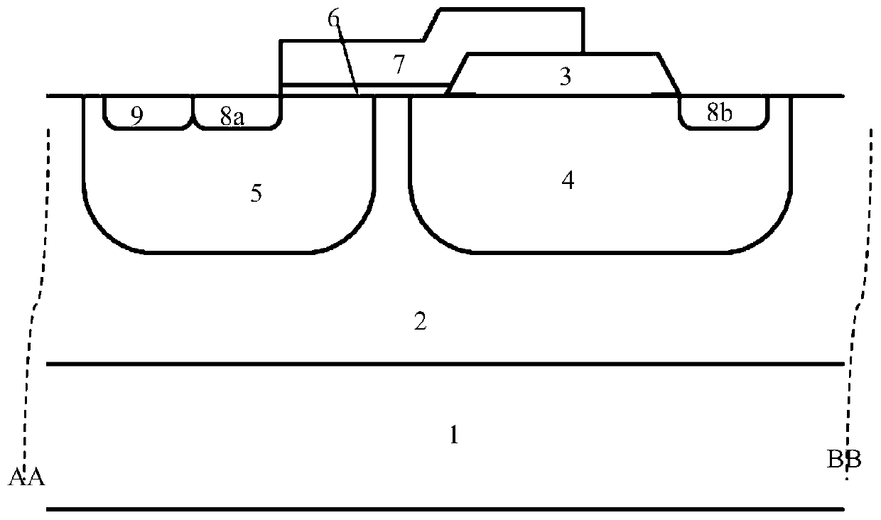
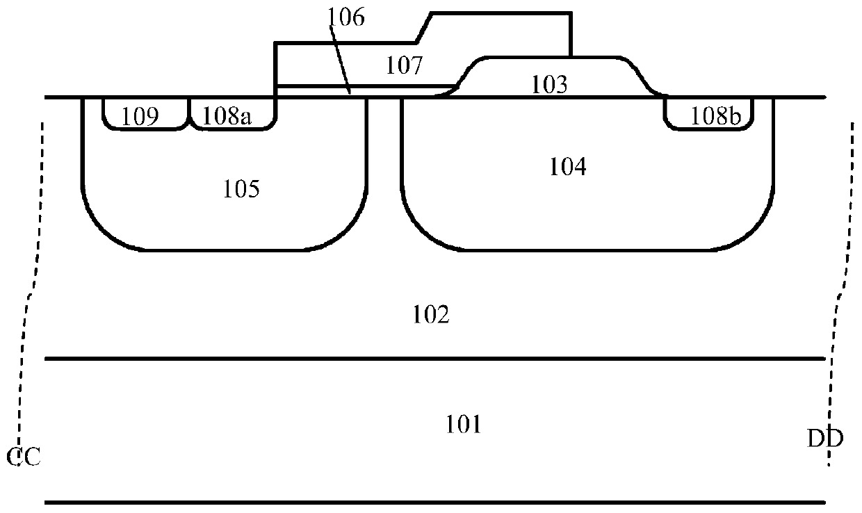
[0054] Such as figure 2 What is shown is a schematic structural diagram of an LDMOS device in an embodiment of the present invention; the LDMOS device in an embodiment of the present invention includes:

[0055] The first epitaxial layer 102 of the second conductivity type has a drift region 104 of the first conductivity type and a body region 105 of the second conductivity type formed in a selected area of ​​the first epitaxial layer 102; the drift regions 104 and The body region 105 is laterally contacted or separated by a distance. Usually multiple LDMOS devices are integrated on the same first epitaxial layer 102, figure 2 Only one LDMOS device located between the dashed line CC and the dashed line DD is shown in the figure. LDMOS devices with the same structure are also formed in other areas outside the dashed line CC and the dashed line DD, and LDMOS devices in other areas outside the dashed line CC and DD Device figure 2 No longer shown in.

[0056] A first buried layer ...


PUM


Abstract

The invention discloses an LDMOS device. A main body part of a drift region field oxide is formed by performing photoetching and etching on a first oxide layer after deposition; the side of the driftregion field oxide is provided with a slowly varying structure, and the slowly varying structure is determined by performing comprehensive anisotropic etching on a second oxide layer after deposition;after deposition, the second oxide layer covers the surface of the main body structure and the surface of a first epitaxial layer outside the main body structure, and forms a slowly varying side above the side of the main body structure; and after the second oxide layer is subjected to comprehensive anisotropic etching, the slowly varying side formed above the side of the main body structure is sunk to form the slowly varying structure, the drift region field oxide contacts a gate dielectric layer through the slowly varying structure, and the electric field strength at the contact location between the drift region field oxide and the gate dielectric layer can be reduced. The invention also discloses a manufacturing method of the LDMOS device. According to the scheme of the invention, thebreakdown voltage of the device can be improved, and the on-resistance of the device can be reduced.

Description

Technical field [0001] The present invention relates to the field of semiconductor integrated circuit manufacturing, in particular to an LDMOS device; the present invention also relates to a manufacturing method of the LDMOS device. Background technique [0002] Double-diffused MOS field effect transistors (Double-diffused MOS) are currently widely used in power management circuits due to their pressure resistance, high current drive capability and extremely low power consumption. DMOS includes vertical double diffused metal oxide semiconductor field effect transistor (VDMOS) and LDMOS (LDMOS). In LDMOS devices, on-resistance is an important indicator. In the BCD process, although LDMOS and CMOS are integrated in the same chip, due to the requirements of high withstand voltage, low characteristic resistance and on-resistance, the conditions of LDMOS in the background region and drift region are shared with the existing process conditions of CMOS Under the premise of, its on-resi...

Claims


Application Information

Patent Timeline
Patent Type & Authority Patents(China)
IPC IPC(8): H01L29/78H01L29/06H01L21/336
CPCH01L29/0603H01L29/0684H01L29/66477H01L29/7816
Inventor 房子荃钱文生
Owner SHANGHAI HUAHONG GRACE SEMICON MFG CORP
Why Eureka
Try Eureka