
Metal contact structure of two-dimensional semiconductor material and method thereof

A two-dimensional semiconductor and metal contact technology, which is applied in the direction of semiconductor devices, semiconductor/solid-state device manufacturing, electrical components, etc., can solve problems such as large influence of properties, large contact resistance, energy level of band gap defects, etc., and achieve simple ohmic contact, Effect of small contact resistance and improved performance

Inactive Publication Date: 2022-04-15
XUZHOU UNIV OF TECH
View PDF0 Cites 0 Cited by
  • Summary
  • Abstract
  • Description
  • Claims
  • Application Information

AI Technical Summary

Problems solved by technology

Ideally, there are no dangling bonds and the surface is passivated, but there are always various defects in the two-dimensional materials prepared by various preparation methods, resulting in a large number of defect energy levels in the forbidden band
[0005] In general, since the two-dimensional material is only composed of the surface, the outside world has too much influence on its intrinsic properties, which is very easy to cause the Fermi pinning effect, and it is difficult to achieve ohmic contact, which is larger than the contact resistance. Therefore, we propose a two-dimensional Metal contact structure of dimensional semiconductor materials and its method to solve the problem

Method used


Image

  • Metal contact structure of two-dimensional semiconductor material and method thereof
  • Metal contact structure of two-dimensional semiconductor material and method thereof

Examples


Embodiment

[0030] A metal contact structure of a two-dimensional semiconductor material, comprising: a substrate, a metal electrode, and a two-dimensional semiconductor material;

[0031] A metal plug is formed over the substrate.

[0032] A metal contact method for a two-dimensional semiconductor material, the steps comprising:

[0033] S1. Depositing a layer of dielectric layer on the substrate, the thickness of the dielectric layer is not more than 0.1 mm;

[0034] S2. Two metal electrodes are arranged at the metal plug, and the two metal electrodes are kept parallel;

[0035] S3, further performing sulfuration treatment on the dielectric layer to form a two-dimensional transition metal compound film;

[0036] S4. A two-dimensional semiconductor material is arranged in the vulcanization treatment area of ​​the dielectric layer, and the two-dimensional semiconductor material accounts for four-fifths of the vulcanization treatment area;

[0037] S5. Use the Kelvin method to calculate...


PUM

PropertyMeasurementUnit
Thicknessaaaaaaaaaa
Thicknessaaaaaaaaaa

Abstract

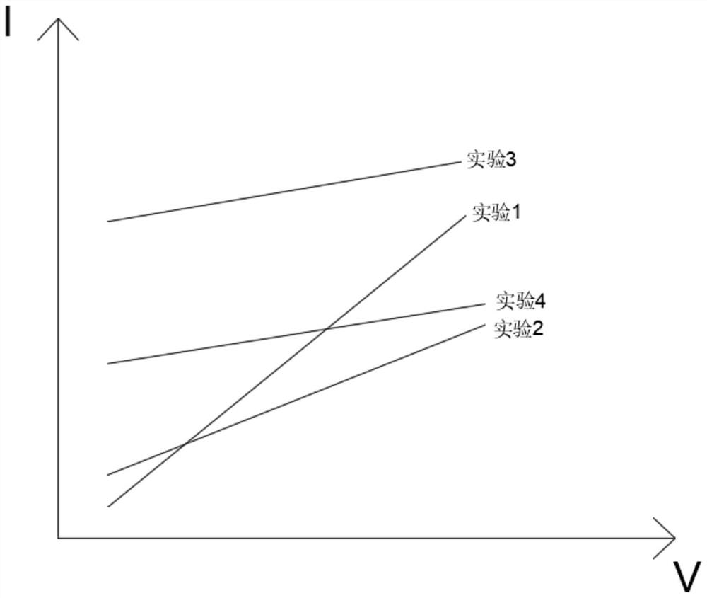
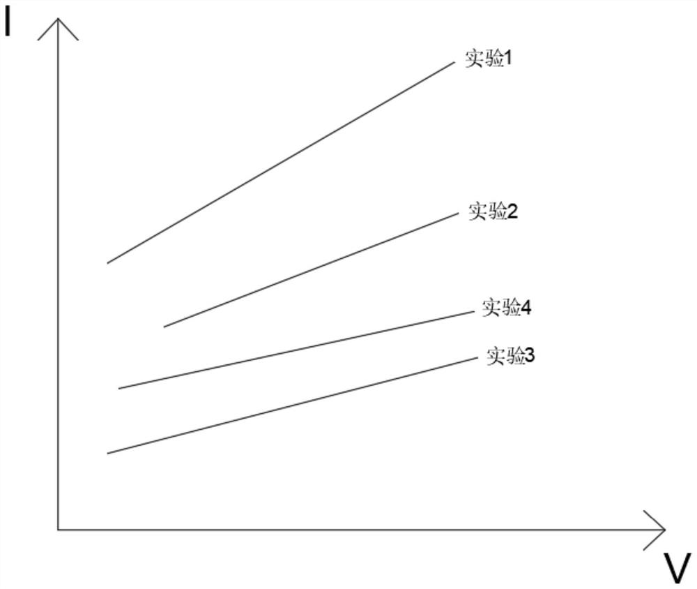
The invention discloses a metal contact method of a two-dimensional semiconductor material. The method comprises the following steps: S1, depositing a dielectric layer on a substrate; s2, arranging a metal electrode at the metal plug; s3, further performing vulcanization treatment on the dielectric layer to form a two-dimensional transition metal compound film; s4, arranging a two-dimensional semiconductor material in the vulcanization treatment area of the dielectric layer; s5, measuring and calculating specific contact resistance by using a Kelvin method, and checking a linear relation of I-V characteristics; and S6, adding a buffer layer between the two-dimensional material and the electrode, continuously changing the thickness and the area of the buffer layer, and repeating the step S5 every time the thickness and the area of the buffer layer are changed. According to the metal contact structure of the two-dimensional semiconductor material and the method thereof, a buffer layer is additionally arranged between the two-dimensional material and the electrode, and the semiconductor two-dimensional material at the contact part is heavily doped, so that the ohmic contact between the two-dimensional semiconductor material and the metal electrode is simple, and the specific contact resistance is small.

Description

technical field [0001] The invention relates to the technical field of semiconductor materials, in particular to a metal contact structure of a two-dimensional semiconductor material and a method thereof. Background technique [0002] Two-dimensional semiconductors refer to materials that are atomically thick and electrons are confined to move in a two-dimensional plane. The quantum confinement effect and weak shielding effect brought about by the reduction of system dimensions endow two-dimensional semiconductors with many novel physical and chemical properties, making them have important application prospects in many fields. Especially in high-performance microelectronic devices, two-dimensional semiconductors have natural advantages. [0003] In the application of two-dimensional semiconductors, the contact with the metal is very important, and the nature of the contact determines the performance of the device, which is one of the hotspots in the research of two-dimensio...

Claims


Application Information

Patent Timeline
IPC IPC(8): H01L29/45H01L21/28H01L21/44
CPCH01L29/45H01L29/452H01L21/28H01L21/44
Inventor 王伟伟
Owner XUZHOU UNIV OF TECH
Learn More