Solar array and preparation method and application thereof
A solar array and printed circuit technology, applied in the field of solar cells, can solve the problems of large volume, weight and complex structure of solar arrays, achieve the effects of multiple payloads, reduce electrical connection procedures, and realize large-scale automated production
- Summary
- Abstract
- Description
- Claims
- Application Information
AI Technical Summary
Problems solved by technology
Method used
Image
Examples
Embodiment 1
[0103] This embodiment is a solar array and its preparation method.
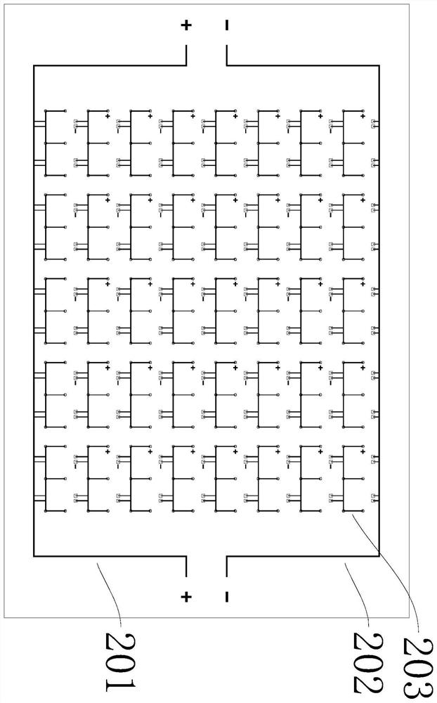
[0104] The solar array of this embodiment includes FPC and flexible CIC cells arranged in sequence.
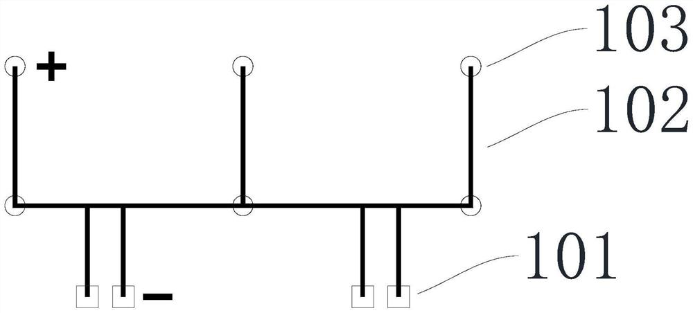
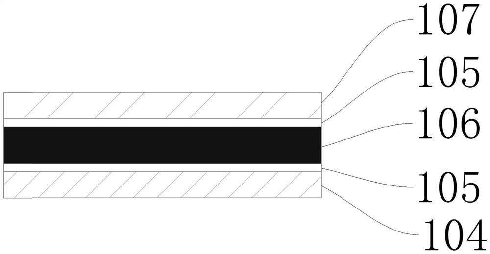
[0105] In this embodiment, some areas of the FPC are arranged sequentially as follows: figure 2 The following structure is shown:
[0106] Bottom layer 104 , glue layer 105 , printed circuit 106 , glue layer 105 and top layer 107 .
[0107] Wherein, the bottom layer 104 is made of polyimide with a thickness of 25 μm;
[0108] The material of the adhesive layer 105 is silica gel, and the thickness is 10 μm;
[0109] The printed circuit layer 106 is made of copper with a thickness of 25 μm;
[0110] The material of the adhesive layer 105 is silica gel, and the thickness is 10 μm;
[0111] The top layer 107 is made of polyimide with a thickness of 25 μm;
[0112] The glue layer 105 is made of silica gel and has a thickness of 10 μm.
[0113] The schematic diagram of the structure of the neutron circuit ...
Embodiment 2
[0135] This embodiment is a solar array and its preparation method.
[0136] The solar array of this embodiment includes FPC and flexible CIC cells arranged in sequence.
[0137] In this embodiment, some areas of the FPC are sequentially set as follows: figure 2 The following structure is shown:
[0138] Bottom layer 104 , glue layer 105 , printed circuit 106 , glue layer 105 and top layer 107 .
[0139] Wherein, the bottom layer 104 is made of polyimide with a thickness of 50 μm;
[0140] The material of the adhesive layer 105 is silica gel, and the thickness is 20 μm;
[0141] The printed circuit layer 106 is made of copper with a thickness of 50 μm;
[0142] The material of the adhesive layer 105 is silica gel, and the thickness is 20 μm;
[0143] The top layer 107 is made of polyimide with a thickness of 50 μm;
[0144] The material of the adhesive layer 105 is silica gel, and the thickness is 20 μm.
[0145] The schematic diagram of the structure of the neutron ci...
PUM
| Property | Measurement | Unit |
|---|---|---|
| thickness | aaaaa | aaaaa |
| thickness | aaaaa | aaaaa |
| thickness | aaaaa | aaaaa |
Abstract
Description
Claims
Application Information
 - R&D
- Intellectual Property
- Life Sciences
- Materials
- Tech Scout
- Unparalleled Data Quality
- Higher Quality Content
- 60% Fewer Hallucinations
Browse by: Latest US Patents, China's latest patents, Technical Efficacy Thesaurus, Application Domain, Technology Topic, Popular Technical Reports.
© 2025 PatSnap. All rights reserved.Legal|Privacy policy|Modern Slavery Act Transparency Statement|Sitemap|About US| Contact US: help@patsnap.com


