Semiconductor laser device

A laser device and semiconductor technology, applied in the laser field, can solve problems such as insufficient optimization

Pending Publication Date: 2022-04-29
BWT BEIJING
View PDF0 Cites 0 Cited by
  • Summary
  • Abstract
  • Description
  • Claims
  • Application Information

AI Technical Summary

Problems solved by technology

State-of-the-art semiconductor lasers are not fully optimized a

Method used


Image

  • Semiconductor laser device
  • Semiconductor laser device
  • Semiconductor laser device

Examples


Embodiment Construction

[0031] Embodiments of the present invention are described in detail below, examples of which are shown in the drawings, wherein the same or similar reference numerals designate the same or similar elements or elements having the same or similar functions throughout. The embodiments described below by referring to the figures are exemplary only for explaining the present invention and should not be construed as limiting the present invention. On the contrary, the embodiments of the present invention include all changes, modifications and equivalents coming within the spirit and scope of the appended claims.

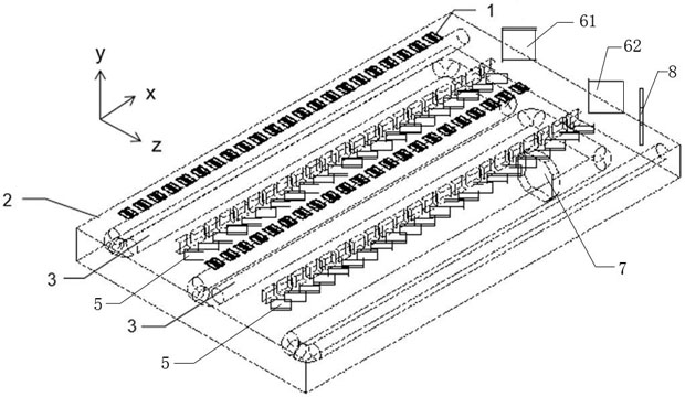
[0032] figure 1 It is a schematic diagram of the overall structure of a semiconductor laser device proposed by an embodiment of the present invention.

[0033] see figure 1 , a semiconductor laser device, including a base plate 2 and a laser array. Wherein, a cooling passage 3 is installed in the bottom plate 2, wherein the cooling passage 3 has a U-shaped pipe, and the...


PUM


Abstract

The invention provides a semiconductor laser device, which comprises a bottom plate, a cooling channel is arranged in the bottom plate, the cooling channel is provided with a U-shaped pipe, and the U-shaped pipe is provided with two straight pipe sections; the laser array comprises a plurality of laser single tubes and small reflectors, the laser single tubes are installed above the position between the two straight tube sections of the U-shaped tube side by side, and the small reflectors are installed at the opposite positions of the laser single tubes side by side and used for irradiating light emitted by the laser single tubes to the beam combining device for space beam combining. According to the semiconductor laser device provided by the invention, the cooling liquid channel is arranged in the bottom plate, the cooling channel is provided with the U-shaped pipe, the U-shaped pipe is provided with the two straight pipe sections, the laser single pipes are arranged above the position between the two straight pipe sections of the U-shaped pipe side by side, and the two straight pipe sections can bring a better cooling effect compared with a single water channel, so that the output power of the laser device can be improved.

Description

technical field [0001] The invention relates to the field of laser technology, in particular to a semiconductor laser device. Background technique [0002] High-power semiconductor lasers are widely used in material processing and pumping solid-state lasers. Heat dissipation is a factor restricting the power-to-mass ratio of semiconductor lasers. Excessive temperature of a single laser tube will affect the performance of the semiconductor laser, or even damage the laser. [0003] In the related art, a single water channel passes under the semiconductor laser single tube array, and the cooling bottom plate is usually made of copper. [0004] During the process of realizing the present invention, the inventors found that there are at least the following problems in the prior art: if the semiconductor laser is to be sufficiently dissipated, the single tube of the semiconductor laser cannot be too concentrated. However, if the single semiconductor laser tube is too dispersed,...

Claims


Application Information

Patent Timeline
IPC IPC(8): H01S5/024H01S5/40
CPCH01S5/02423H01S5/02469H01S5/4075
Inventor 陈晓华郭渭荣王宝华时敏李娟董晓培郭方君玥
Owner BWT BEIJING
Why Eureka
Try Eureka