Flip-chip bonding method for preventing adhesion and pseudo soldering

A welding method and flip-chip welding technology, which is applied to semiconductor devices, electrical components, circuits, etc., can solve problems such as easy adhesion or virtual welding, and achieve the effect of reducing the difficulty of the welding process

Pending Publication Date: 2022-05-03
深圳市潜力创新科技有限公司
View PDF0 Cites 0 Cited by
  • Summary
  • Abstract
  • Description
  • Claims
  • Application Information

AI Technical Summary

Problems solved by technology

[0003] The main purpose of the present invention is to propose a flip-chip welding method for preventing virtual soldering, aiming at solving the problem of easy adhesion or virtual soldering in the current flip-chip soldering technology

Method used


Image

  • Flip-chip bonding method for preventing adhesion and pseudo soldering
  • Flip-chip bonding method for preventing adhesion and pseudo soldering
  • Flip-chip bonding method for preventing adhesion and pseudo soldering

Examples


Embodiment Construction

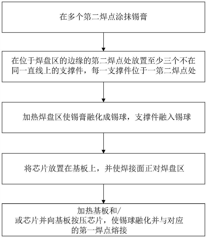
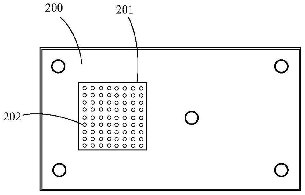
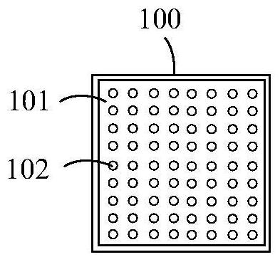
[0025] The following will clearly and completely describe the technical solutions in the embodiments of the present invention with reference to the accompanying drawings in the embodiments of the present invention. Obviously, the described embodiments are only part of the embodiments of the present invention, not all of them. Based on the embodiments of the present invention, all other embodiments obtained by persons of ordinary skill in the art without creative efforts fall within the protection scope of the present invention.

[0026] It should be noted that if there is a directional indication (such as up, down, left, right, front, back...) in the embodiment of the present invention, the directional indication is only used to explain the position in a certain posture (as shown in the accompanying drawing). If the specific posture changes, the directional indication will also change accordingly.

[0027] In addition, if there are descriptions involving "first", "second" and ...


PUM

PropertyMeasurementUnit
thicknessaaaaaaaaaa
diameteraaaaaaaaaa

Abstract

The flip-chip bonding method for preventing adhesion and pseudo soldering is used for welding a chip to a substrate, the welding surface of the chip is provided with a plurality of first welding spots, the substrate is provided with a bonding pad area corresponding to the welding surface, and the bonding pad area is provided with a plurality of second welding spots corresponding to the first welding spots. The flip-chip bonding method comprises the following steps: smearing solder paste on the plurality of second welding spots; at least three supporting pieces which are not on the same straight line are placed at second welding spots located at the edge of the bonding pad area, and each supporting piece is located at the corresponding second welding spot; heating the bonding pad area to melt the solder paste into a solder ball, and fusing the supporting piece into the solder ball; placing a chip on the substrate, and enabling a welding surface to directly face the bonding pad area; heating the substrate and/or the chip, and pressing the chip to the substrate, so that the solder balls are melted and welded with the corresponding first welding spots; the supporting piece abuts against the chip and the substrate so as to limit the distance between the chip and the substrate. According to the technical scheme, the problem that pseudo soldering and adhesion are prone to being generated in flip-chip bonding can be solved.

Description

technical field [0001] The invention relates to the field of welding technology, in particular to a flip-chip welding method for preventing sticking and virtual welding. Background technique [0002] Flip-chip welding technology refers to a technology in which the IC chip faces down and is directly interconnected with the packaging shell or the wiring substrate, also known as the flip-chip welding technology. Flip-chip soldering has short interconnection lines, small parasitic capacitance and inductance, and the electrodes of the chip can be arranged arbitrarily on the chip surface, and the packaging density is high. Welding of high-frequency, high-speed large-scale integrated circuits, ultra-large-scale integrated circuits and application-specific integrated circuits. However, because the welding surface is facing downward, the welding state of the welding surface cannot be observed intuitively, and it is prone to sticking or false welding. Especially in the maintenance o...

Claims


Application Information

Patent Timeline
Patent Type & Authority Applications(China)
IPC IPC(8): H01L21/603
CPCH01L24/81H01L2224/81007H01L2224/81203
Inventor 杨长顺张志衡薛仁峰张阳
Owner 深圳市潜力创新科技有限公司
Why Eureka
Try Eureka