Optical communication module and upgrading equipment

An optical communication module and optical communication technology, applied in the direction of equipment, optics, instruments, etc. that apply the electrical recording process of charge graphics, can solve the problem of packaging sealing, impact of anti-collision performance, large penetrability window, and inconvenient reading of chips Problems such as writing and upgrading to achieve the effect of reducing fixed difficulty and reducing waste

Pending Publication Date: 2022-05-06
APEX MICROELECTRONICS CO LTD
View PDF0 Cites 0 Cited by
  • Summary
  • Abstract
  • Description
  • Claims
  • Application Information

AI Technical Summary

Problems solved by technology

On the other hand, even if there is a window on the packaging box, the consumable chip can be powered through this window to read, write, and upgrade, but different consumable boxes may have different shapes, and the installation position of the chip may not be convenient for reading and writing. upgrade
Moreover, in order to facilitate the reading, writing and upgrading of the chip, it may be necessary to open a larger penetrability window, which will have a greater impact on the sealing and anti-collision performance of the package.
For the package where the consumable chip is far away from the outside of the packaging box, the read-write and upgrade equipment needs to be equipped with a slender test head, and the contacts on the chip are small. To ensure stable electrical contact, the chip must be firmly fixed, but , it is difficult to fix consumable chips outside the packaging box

Method used


Image

  • Optical communication module and upgrading equipment
  • Optical communication module and upgrading equipment
  • Optical communication module and upgrading equipment

Examples


Embodiment 1

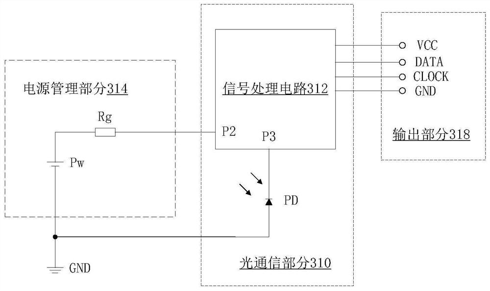
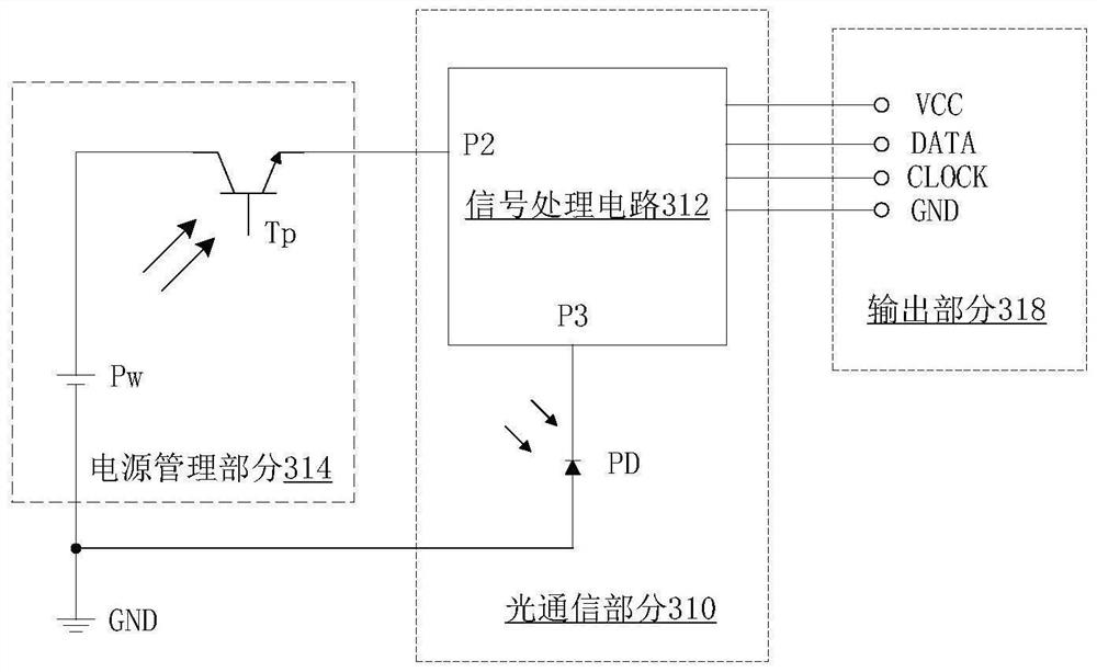
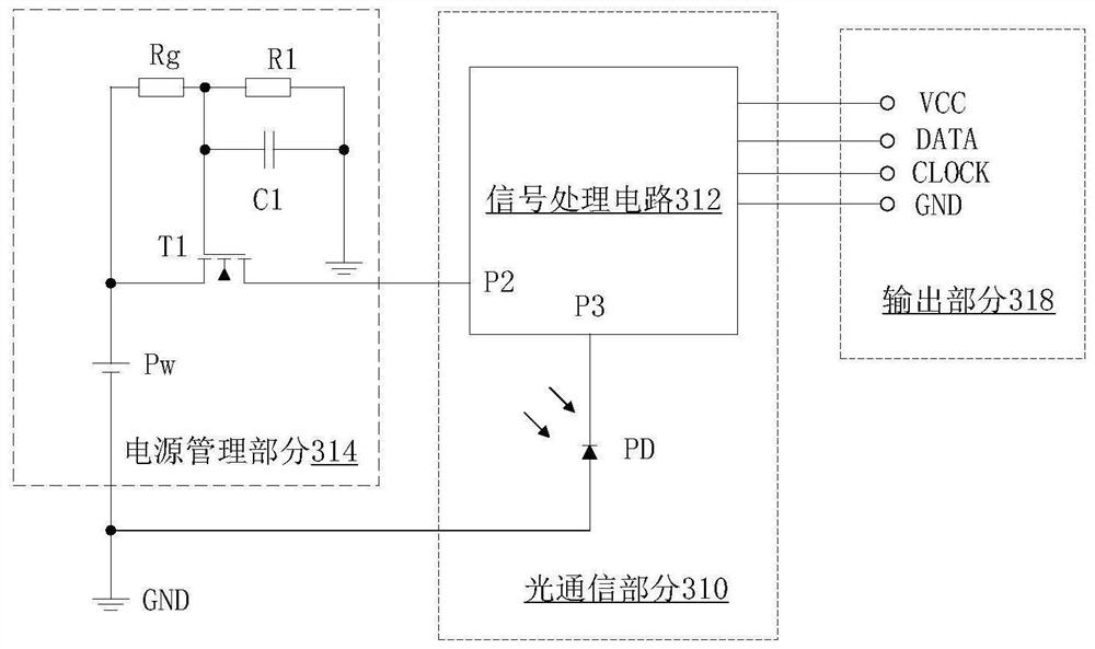
[0039] The present invention provides a solution for reading and writing data to consumable chips and upgrading consumable chips without opening a large window on the packaging box, which can maintain the sealing of the packaging box and reduce the difficulty of fixing consumables without strict Fixed consumable chips.

[0040] Such as figure 1As shown, the optical communication module provided by the present invention includes a power management part 314, an optical communication part 310 and an output part 318. The power management part 314 is configured (for) to communicate with the optical The part 310 provides power; the optical communication part 310 is used to start working when receiving the power, receives the optical communication signal and converts the optical communication signal into a decoding signal; the output part is used to output the power and the decoding signal externally, if the optical communication module is powered Connected to the consumable chip, t...


PUM


Abstract

The invention provides an optical communication module and a chip comprising the optical communication module, the optical communication module comprises a power supply management part, an optical communication part and an output part, the power supply management part is configured to provide a power supply for the optical communication part after receiving a preset optical signal; the optical communication part is configured to receive an optical communication signal and convert the optical communication signal into a decoding signal; the output portion is configured to output the power supply and the decoded signal to the outside. According to the invention, the packaging box does not need to be dismantled when the chip is upgraded, and the optical signal is used as a signal for starting the battery of the optical communication module, so that the electric quantity of the battery of the optical communication module cannot be used in advance, the waste of the electric quantity is reduced, and the battery can be provided for a consumable chip and other power-free devices for long-time optical communication.

Description

technical field [0001] The invention relates to a power-saving optical communication module, which can conveniently rewrite and upgrade the information of consumable chips and other devices without power supply through optical signals. Background technique [0002] Printing equipment (such as inkjet printers, laser printers, all-in-one machines, etc.) needs consumables boxes such as ink cartridges, powder cartridges, and toner cartridges during the printing process, wherein ink is contained in the ink cartridges, and ink is contained in the toner cartridges and toner cartridges. Contains toner. These printing consumables have a shorter lifespan than printing equipment, so users need to purchase and replace consumable cartridges frequently during use. These consumable boxes are generally placed in packaging boxes and sold in the form of packages after being packaged. [0003] In order to record the usage of the consumables box installed in the printing device and to identif...

Claims


Application Information

Patent Timeline
Patent Type & Authority Applications(China)
IPC IPC(8): G03G21/14G03G15/08G03G15/00
CPCG03G21/14G03G15/0863G03G15/5075
Inventor 陈浩
Owner APEX MICROELECTRONICS CO LTD
Why Eureka
Try Eureka