Printed circuit board and manufacturing method thereof

A printed circuit board and manufacturing method technology, applied in the directions of printed circuit manufacturing, laminated printed circuit boards, printed circuits, etc., can solve the problems of different branch or signal width, low work efficiency, inconvenient operation, etc., to reduce processing Steps, testing convenience, and the effect of improving work efficiency

Pending Publication Date: 2022-05-06
上海卓冬应用技术工程有限公司
View PDF0 Cites 0 Cited by
  • Summary
  • Abstract
  • Description
  • Claims
  • Application Information

AI Technical Summary

Problems solved by technology

In the actual production process, it is impossible for many electronic products to be successful at one time, so repeated testing, debugging, and retesting are required; It will cause a lot of unnecessary troubles, the branch or signal width is different; at the same time, in the preparation of the circuit board, the multi-layer composition must be pressed together. The existing method uses two iron plates to fix and clamp the PVB, but the operation is inconvenient. Connect multiple bolts between two iron plates for assembly and pressing, which is laborious to use and low in work efficiency; in view of the above problems, we propose a printed circuit board and a method for manufacturing a printed circuit board

Method used


Image

  • Printed circuit board and manufacturing method thereof
  • Printed circuit board and manufacturing method thereof
  • Printed circuit board and manufacturing method thereof

Examples


Embodiment 1

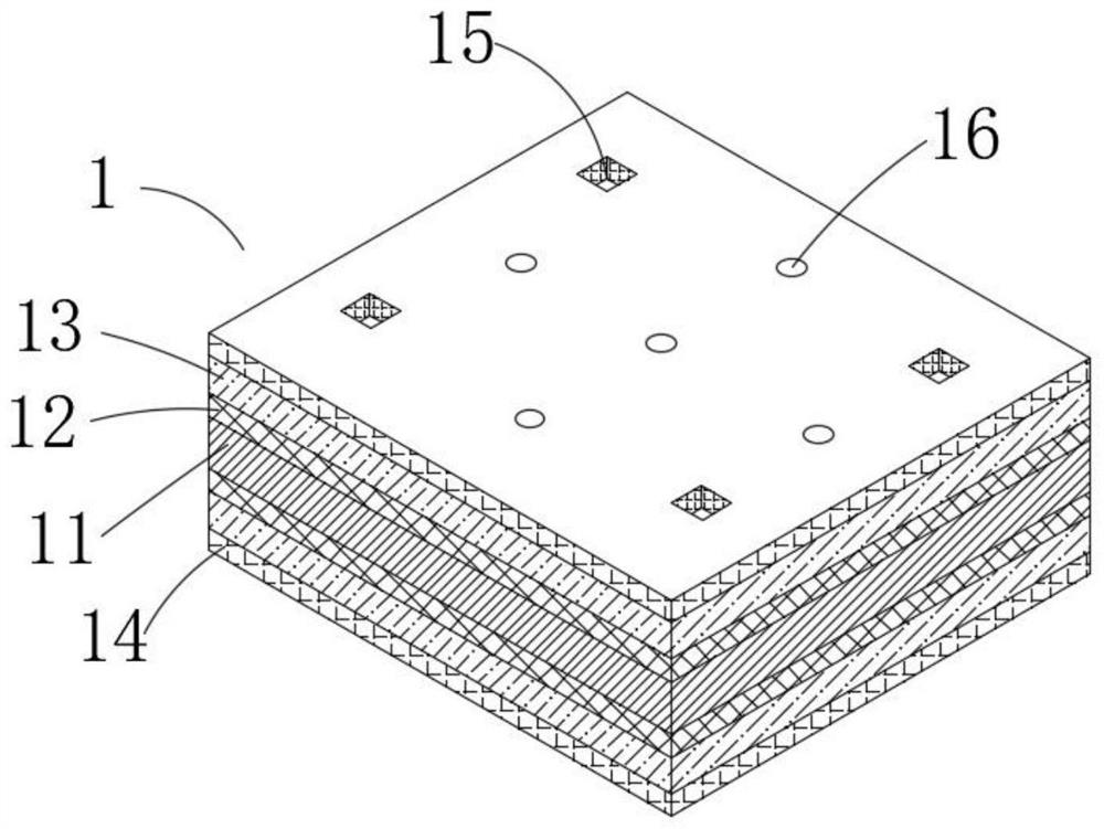
[0027] Such as figure 1 As shown, a printed circuit board proposed by the present invention includes a circuit board body 1, and the circuit board body 1 includes a core board 11. Prepregs 12 are provided on both sides of the core board 11, and copper foil is connected to the other side of the prepreg 12. 13. An aluminum plate 14 is provided on the other side of the copper foil 13. A blind hole 15 is opened on the aluminum plate 14. A signal hole 16 is opened on the circuit board body 1. The signal hole 16 runs through the circuit board body 1, and the inside of the signal hole 16 is coated with Has an antioxidant layer.

[0028] In this embodiment, a printed circuit board is composed of a core board 11, a prepreg 12, a copper foil 13, and an aluminum plate 14. The setting of the signal hole 16 improves the stability of the circuit board body 1 when performing signal transmission detection, and the signal transmission is stable. The difference is reduced.

Embodiment 2

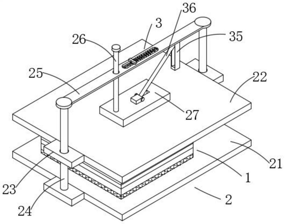
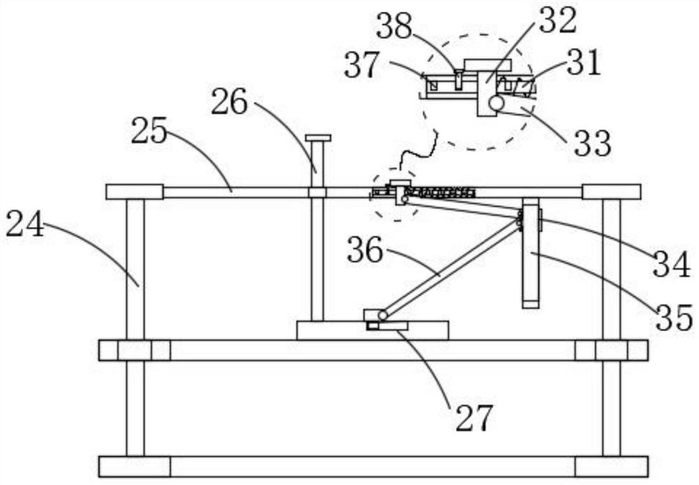
[0030] Such as Figure 2-3 As shown, a printed circuit board proposed by the present invention, compared with the first embodiment, this embodiment also includes: a circuit board body 1, the circuit board body 1 uses a pressing mechanism 2 in the pressing process, and the pressing An adjustment mechanism 3 is provided on the mechanism 2. Furthermore, the present invention also proposes a method for manufacturing a printed circuit board, which includes the following steps:

[0031] S1. Material preparation: pre-preparing and processing the component parts of each layer of the circuit board, the component parts include the core board 11, the prepreg 12, the copper foil 13 and the aluminum plate 14;

[0032] S2. Punching and pressing: laying and stacking the core board 11, the prepreg 12, the copper foil 13 and the aluminum plate 14 in sequence, and positioning and pressing through the pressing mechanism 2;

[0033] S3. Hole treatment: drilling the circuit board body 1 with a dr...


PUM


Abstract

The invention relates to the technical field of electronic product processing, in particular to a printed circuit board. According to the technical scheme, the circuit board comprises a circuit board body, the circuit board body comprises a core plate, prepregs are arranged on the two sides of the core plate, copper foil is connected to the other sides of the prepregs, an aluminum plate is arranged on the other side of the copper foil, blind holes are formed in the aluminum plate, and signal holes are formed in the circuit board body. The invention further discloses a manufacturing method of the printed circuit board. The manufacturing method comprises the following steps: S1, preparing materials; s2, punching and pressing; s3, hole treatment; and S4, transfer electroplating. The printed circuit board is convenient to test, high in signal transmission stability, high in signal transmission accuracy, simple in pressing mode, capable of reducing processing steps and improving processing efficiency, suitable for processing and using circuit boards with different layer numbers, capable of improving using flexibility and universality and suitable for application and popularization.

Description

technical field [0001] The invention relates to the technical field of electronic product processing, in particular to a printed circuit board and a method for manufacturing the printed circuit board. Background technique [0002] The printed circuit board is mainly composed of two types of materials: insulating substrate and conductor, which play the role of supporting, interconnecting and some circuit components in electronic equipment. Electronic components such as integrated circuits and resistors and capacitors can only function in this whole if they have a foothold on the printed circuit board and are connected by wires. The printed circuit board is the skeleton that supports components and connects electrical signals. In the actual production process, it is impossible for many electronic products to be successful at one time, so repeated testing, debugging, and retesting are required; It will cause a lot of unnecessary troubles, the branch or signal width is differe...

Claims


Application Information

Patent Timeline
Patent Type & Authority Applications(China)
IPC IPC(8): H05K1/02H05K3/00
CPCH05K1/0268H05K3/0058
Inventor 周晓峰
Owner 上海卓冬应用技术工程有限公司
Why Eureka
Try Eureka