Supercharge Your Innovation With Domain-Expert AI Agents!

Chip surface defect parallel detection method based on improved convolution variational auto-encoder

An autoencoder and detection method technology, applied in image coding, neural learning methods, instruments, etc., can solve the problem of short detection time, and achieve the effect of reducing manpower and material resources, reducing defect detection time, and reducing labor and time costs.

Pending Publication Date: 2022-05-10
XIDIAN UNIV
View PDF0 Cites 1 Cited by
  • Summary
  • Abstract
  • Description
  • Claims
  • Application Information

AI Technical Summary

Problems solved by technology

[0003] The invention improves the problem that chip surface defect detection still needs to be intelligent in the prior art, and provides a chip surface defect parallel detection method based on improved convolutional variational autoencoder with short detection time and comprehensive detection

Method used


Image

  • Chip surface defect parallel detection method based on improved convolution variational auto-encoder
  • Chip surface defect parallel detection method based on improved convolution variational auto-encoder

Examples


Embodiment Construction

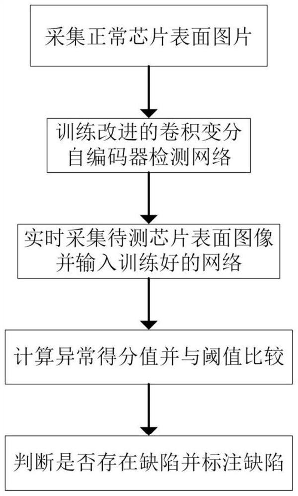
[0015] The method for parallel detection of chip surface defects based on the improved convolutional variational autoencoder of the present invention will be further described below in conjunction with the accompanying drawings and specific embodiments: This embodiment includes the following steps:

[0016] S1, chip image acquisition and preprocessing, S2, construction and training of an improved convolutional variational autoencoder, S3, real-time defect detection of the chip to be tested.

[0017] S1 consists of the following steps:

[0018] S1.1. Use the high-definition camera module, the host image processing module and the lighting module to collect and store images for subsequent image processing. In addition, it is equipped with a defect sound and light alarm module to prompt the detection of defective chips. Using a CCD camera, two LED array light sources intersect for fan-shaped dark field illumination.

[0019] S1.2. Collect the surface image of a normal chip, decom...


PUM


Abstract

The invention discloses a chip surface defect parallel detection method based on an improved convolution variational auto-encoder. The problem that chip surface defect detection still needs to be intelligent in the prior art is solved. The method comprises the following steps: step 1, acquiring and preprocessing a chip image; step 2, constructing and training an improved convolution variational auto-encoder; and step 3, performing real-time defect detection on the chip to be detected. According to the method, a traditional variational auto-encoder is partially improved, all defects different from those of a normal sample can be detected only by using the normal sample for unsupervised training and without labeled defect sample data, manpower and material resources are reduced, meanwhile, the original image is decomposed into a plurality of sub-images by the method and then the sub-images are processed in parallel, and the detection accuracy is improved. And various defects on the surface of the chip can be efficiently and quickly detected at low cost.

Description

technical field [0001] The invention relates to the technical field of computer vision applied to chip screening, in particular to a method for parallel detection of chip surface defects based on an improved convolutional variational autoencoder. Background technique [0002] The purpose of chip surface defect detection is to eliminate defective chips with surface defects such as character defects, pin defects, and surface scratches on the production line, which is the key to controlling product quality. Traditional defect detection methods based on explicit feature extraction require manual design for feature extraction, which is time-consuming; while most current surface defect detection methods based on deep learning are based on supervised learning of a large number of defect samples, requiring a large number of well-labeled training Samples are learned end-to-end, but it is very difficult to collect a large number of defect samples. The accidental and random nature of d...

Claims


Application Information

Patent Timeline
IPC IPC(8): G06T7/00G06T9/00G06N3/08G06N3/04
CPCG06T7/0004G06T9/002G06N3/088G06T2207/20081G06N3/048G06N3/045
Inventor 任获荣马振韩健平续斌焦小强张志新
Owner XIDIAN UNIV
Features
  • R&D
  • Intellectual Property
  • Life Sciences
  • Materials
  • Tech Scout
  • Unparalleled Data Quality
  • Higher Quality Content
  • 60% Fewer Hallucinations
Learn More