
Automatic test machine control system suitable for PCB ICT

An automatic testing machine, PCB board technology, used in electronic circuit testing, measuring electricity, measuring devices, etc.

Pending Publication Date: 2022-05-20
深圳市微特精密科技股份有限公司
View PDF0 Cites 1 Cited by
  • Summary
  • Abstract
  • Description
  • Claims
  • Application Information

AI Technical Summary

Problems solved by technology

[0004] The invention provides an automatic testing machine control system suitable for PCB board ICT, which is used to solve the problem that multiple types of PCB board tests can be performed when PCB boards are tested

Method used


Image

  • Automatic test machine control system suitable for PCB ICT
  • Automatic test machine control system suitable for PCB ICT
  • Automatic test machine control system suitable for PCB ICT

Examples


Embodiment 1

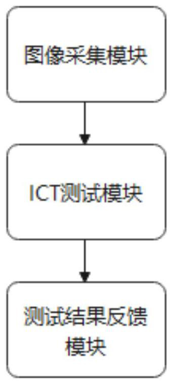
[0053] Embodiments of the present invention provides an automatic test machine control system suitable for PCB board ICT, such as Figure 1 shown, including:

[0054] Image acquisition module: used to position the PCB board, and the PCB board for all-round surround image acquisition, acquisition of PCB board images;

[0055] ICT test module: for automatically identifying the components of the PCB board image, segmenting the area according to the components, determining the component partition, and automatically comparing and calculating the difference with the standard component partition image, and generating the partition automatic test results;

[0056] Test result feedback module: used to receive the automatic test results of the partition, and summarize the automatic test results of all partitions, and generate the total results for feedback.

[0057] The above technical solution works as follows:

[0058] In the prior art of the present invention, the PCB board automatic detect...

Embodiment 2

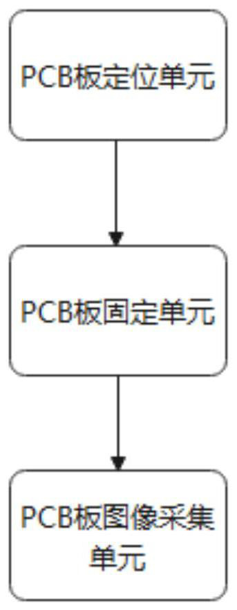
[0061]As an embodiment of the present invention: e.g., Figure 2 As shown, the image acquisition module, comprising:

[0062] PCB board positioning unit: used to establish an infrared coordinate system on the PCB board placement table, locate the PCB board, and enter the vertex coordinates of the PCB board;

[0063] PCB board fixing unit: used to fix the edge of the PCB board by the gripper, and move the camera gimbal for mobile shooting;

[0064] PCB board image acquisition unit: Used to acquire images at equal intervals and store PCB board images to the PCB board library.

[0065] The above technical solution works as follows:

[0066] In the prior art of the present invention, by installing a PCB board magnetic adsorption device on the pcB board placement table, fixing the PCB board, tilting and rotating the PCB board placement table for PCB board image shooting acquisition, but the specifications of the PCB board are inconsistent, some PCB boards are relatively light, can be ti...

Embodiment 3

[0069] As an embodiment of the present invention: the ICT test module comprising:

[0070] ICT identification unit: for scanning the PCB board image, determining the ICT parameters of the PCB board; wherein, the ICT parameters include: the contour size of the PCB board, component position, circuit wiring, fusion solder joint position;

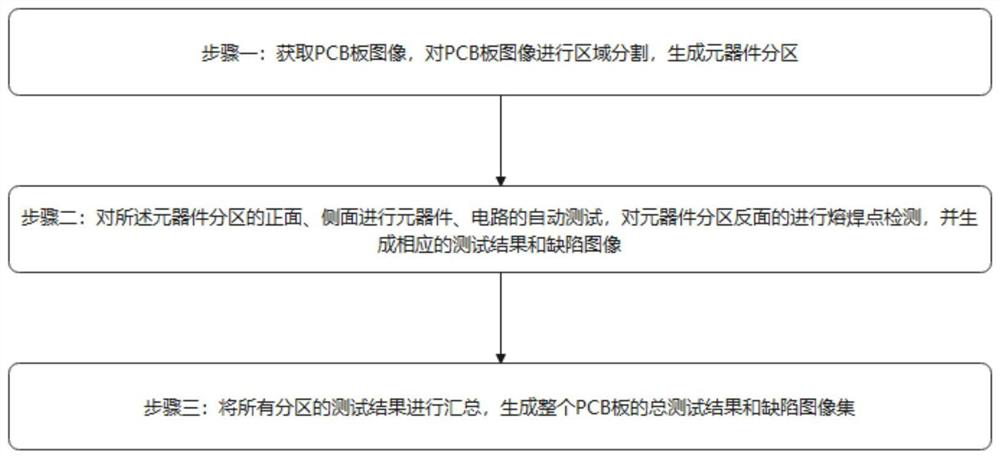
[0071]ICT partitioning unit: used to rectangular segment the front and side of the PCB board centered on the position of the component, confirm the component partition, and combine the component partition, detect whether the image is complete after the combination, if the image is complete, then carry out the partition automatic test, otherwise, re-divide the area;

[0072] Partition test unit: used to summarize all component partition images on the front and side of the PCB board, build a stereoscopic image of the component partition, conduct preliminary automatic detection and accurate automatic detection of the stereoscopic image and the standar...


PUM


Abstract

The invention provides an ICT automatic test machine control system suitable for a PCB, and the system comprises an image collection module which is used for positioning the PCB, carrying out the all-dimensional surrounding image collection of the PCB, and obtaining a PCB image, and an ICT test module which is used for automatically recognizing a component of the PCB image, carrying out the region segmentation according to the component, determining a component subregion, and carrying out the detection of the component subregion. The partition test module is used for carrying out partition test on the PCB image and carrying out automatic comparison and difference calculation with a standard component partition image to generate a partition automatic test result, and the test result feedback module is used for receiving the partition automatic test result, summarizing the automatic test results of all partitions and generating and feeding back a total result. The limitation of the model of the PCB is avoided, and the PCB of different models can be automatically tested.

Description

Technical field [0001] The present invention relates to the field of automatic testing machine technology, in particular to a kind of ICT automatic testing machine control system suitable for PCB boards Background [0002] At present, China's electronic information products manufacturing industry is huge, microelectronic products with the rise of electronic manufacturing industry rapid development, followed by microelectronic products production test equipment also began to gradually mature, PCB board detection is one of the important detection of microelectronic products, according to different PCB boards, factories will take different detection methods and devices. [0003] For example, the papers Gil, I, Femandez-Garcia, R. Electromagnetic interference reductionin printed circuit boards by using metamaterials:a conduction and radiationimpact analysis[J]. Joumal of Electromagnetic Waves and Applications, 2014, Pages 378-388 commonly used detection methods mentioned are: (1) man...

Claims


Application Information

Patent Timeline
IPC IPC(8): G01R31/28
CPCG01R31/2806
Inventor 程志勇
Owner 深圳市微特精密科技股份有限公司
Learn More