
Simulation method and simulation model structure of super-junction MOSFET (Metal Oxide Semiconductor Field Effect Transistor) device

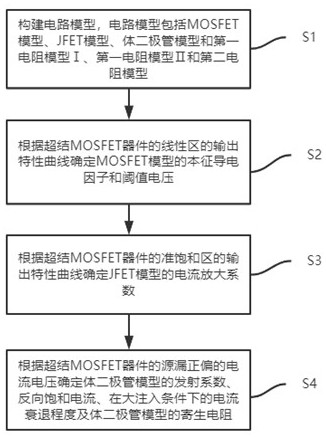
A simulation method and simulation model technology, applied in the fields of instrumentation, calculation, electrical digital data processing, etc., can solve the problem that the MOSFET model cannot accurately describe super-junction MOSFET devices, etc., and achieve the effect of high simulation accuracy

Active Publication Date: 2022-06-03
VANGUARD SEMICON CORP
View PDF13 Cites 1 Cited by
  • Summary
  • Abstract
  • Description
  • Claims
  • Application Information

AI Technical Summary

Problems solved by technology

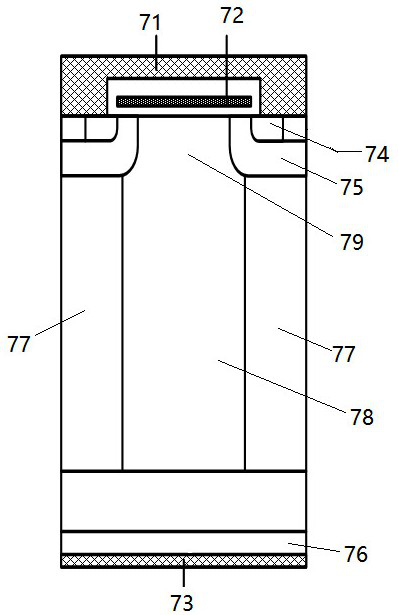
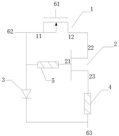
[0004] The present invention aims at the problem that traditional MOSFET models cannot accurately describe the characteristics of super-junction MOSFET devices. On the one hand, it provides a simulation method for super-junction MOSFET devices; on the other hand, it provides a model structure of super-junction MOSFET devices. The specific technical scheme is as follows

Method used


Image

  • Simulation method and simulation model structure of super-junction MOSFET (Metal Oxide Semiconductor Field Effect Transistor) device
  • Simulation method and simulation model structure of super-junction MOSFET (Metal Oxide Semiconductor Field Effect Transistor) device
  • Simulation method and simulation model structure of super-junction MOSFET (Metal Oxide Semiconductor Field Effect Transistor) device

Examples


Embodiment Construction

[0024] Example embodiments will now be described more fully with reference to the accompanying drawings. Example embodiments, however, can be embodied in various forms and should not be construed as limited to the embodiments set forth herein; rather, these embodiments are provided so that this disclosure will be thorough and complete, and will fully convey the concept of example embodiments to those skilled in the art. The same reference numerals in the drawings denote the same or similar parts, and thus their repeated descriptions will be omitted.

[0025] Furthermore, the described features, structures, or characteristics may be combined in any suitable manner in one or more embodiments. In the following description, numerous specific details are provided in order to give a thorough understanding of the embodiments of the present disclosure. However, one skilled in the art will appreciate that the technical solutions of the present disclosure may be practiced without one ...


PUM


Abstract

The invention relates to a simulation method and a simulation model structure of a super junction MOSFET device, and the simulation method comprises the steps: building a circuit model which comprises an MOSFET model, a JFET model, a body diode model, a first resistor model I, a first resistor model II and a second resistor model; the drain electrode of the MOSFET model is connected with the source electrode of the JFET model; the source electrode of the MOSFET model is respectively connected with the grid electrode of the JFET model and the positive electrode of the body diode model; the first end of the first resistance model I is connected with the drain electrode of the JFET model, and the second end of the first resistance model I is connected with the first end of the first resistance model II; the second end of the first resistance model II is connected with the cathode of the body diode model. The simulation method provided by the invention can effectively simulate the characteristics of the super-junction MOSFET device in each working area, and the simulation accuracy is high.

Description

technical field [0001] The invention relates to the field of simulation of semiconductor devices, in particular to a simulation method and simulation model structure of a super-junction MOSFET device. Background technique [0002] In recent years, thanks to the rapid development of computer technology, circuit simulation has become more and more familiar and used by people, and has gradually become an indispensable key link in circuit design. SPICE (Simulation Program for Integrated Circuits Emphasis) was developed by the Electronic Research Laboratory of the University of California, Berkeley in 1975. Integrated circuit design, PCB board level and system level design are inseparable from SPICE simulation. The device model is regarded as a bridge connecting circuit design and process production. With the help of circuit simulator, a large number of virtual experiments and simulations can be performed using the device model to predict the performance of the circuit, thereby i...

Claims


Application Information

Patent Timeline
Patent Type & Authority Applications(China)
IPC IPC(8): G06F30/367
CPCG06F30/367Y02E60/00
Inventor 李伟聪姜春亮雷秀芳林泳浩
Owner VANGUARD SEMICON CORP
Learn More