
Light-emitting element for display and LED display device having same

A light-emitting element and display substrate technology, which is applied in the direction of electrical components, semiconductor devices, electric solid-state devices, etc., can solve the problems that the display device is difficult to match the RGB mixing ratio, and the luminous intensity of the blue LED is high.

Pending Publication Date: 2022-06-07
SEOUL VIOSYS CO LTD
View PDF0 Cites 0 Cited by
  • Summary
  • Abstract
  • Description
  • Claims
  • Application Information

AI Technical Summary

Problems solved by technology

However, since currently used LED chips generally have a relatively high luminous intensity of blue LEDs compared to other LEDs, there is a problem that it is difficult for display devices using LED chips to match the RGB mixing ratio.

Method used


Image

  • Light-emitting element for display and LED display device having same
  • Light-emitting element for display and LED display device having same
  • Light-emitting element for display and LED display device having same

Examples


Embodiment Construction

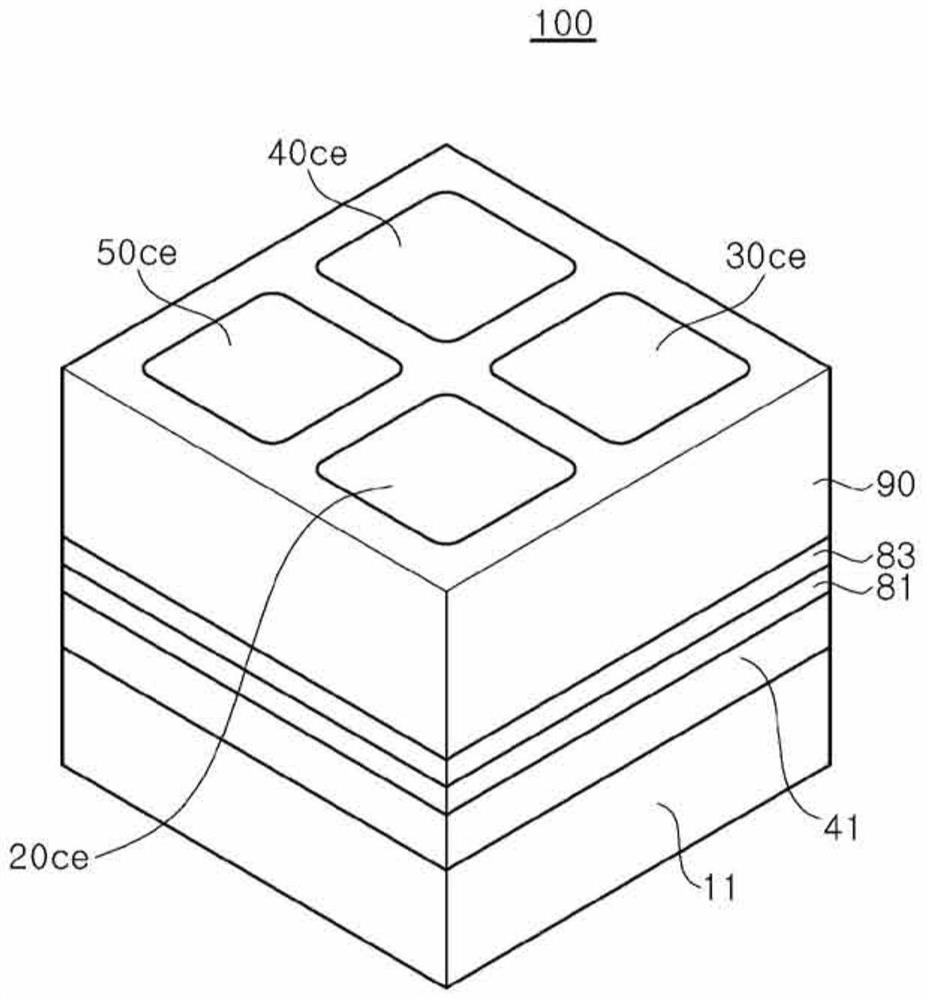
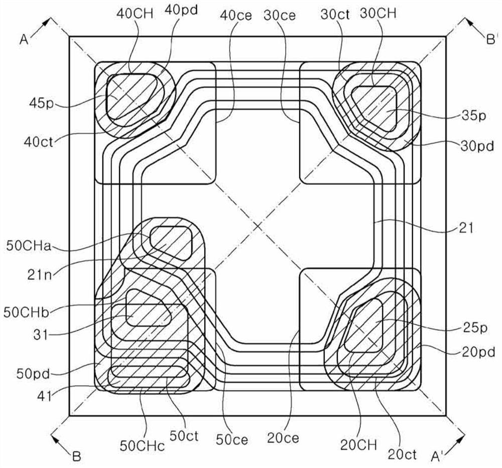
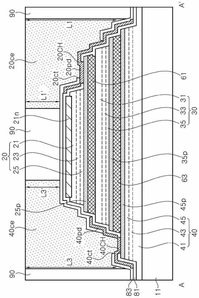
[0025] Hereinafter, embodiments of the present disclosure will be described in detail with reference to the accompanying drawings. In order to fully convey the idea of ​​the present disclosure to those skilled in the art to which the present disclosure pertains, the embodiments introduced below are provided as examples. Therefore, the present disclosure is not limited to the embodiments described below, but may be embodied in other forms. In addition, in the drawings, the width, length, thickness, and the like of constituent elements may be exaggerated for convenience of explanation. In addition, when it is stated that one component is located "on" or "on" another component, it includes not only the case where each part is "directly" located on the "upper" or "on" of the other component, but also includes the relationship between each component and the other components. A case where another component is sandwiched between another component. The same reference numerals denote...


PUM

PropertyMeasurementUnit
light emitting areaaaaaaaaaaa
thicknessaaaaaaaaaa
thicknessaaaaaaaaaa

Abstract

The light-emitting element according to an embodiment includes a first light-emitting stack, a second light-emitting stack, and a third light-emitting stack, each of the first light emitting stack, the second light emitting stack, and the third light emitting stack includes a first conductive type semiconductor layer, a second conductive type semiconductor layer, and an active layer disposed between the first conductive type semiconductor layer and the second conductive type semiconductor layer; a first lower contact electrode in ohmic contact with the first light emitting stack; a second lower contact electrode in ohmic contact with the second conductive type semiconductor layer of the second light emitting stack; and a third lower contact electrode in ohmic contact with the second conductive type semiconductor layer of the third light emitting stack, in which the second light emitting stack is disposed between the first light emitting stack and the third light emitting stack, and the first lower contact electrode is in ohmic contact with the second conductive type semiconductor layer of the third light emitting stack. The first lower contact electrode is arranged between the first light-emitting stack and the second light-emitting stack, and the second lower contact electrode and the third lower contact electrode are arranged between the second light-emitting stack and the third light-emitting stack, the first lower contact electrode, the second lower contact electrode, and the third lower contact electrode include a transparent conductive oxide layer, and a thickness of the second lower contact electrode or the third lower contact electrode is greater than a thickness of the first lower contact electrode.

Description

technical field [0001] The present disclosure relates to a light-emitting element for display and an LED display device having the same. Background technique [0002] As inorganic light sources, light emitting diodes are widely used in various fields such as display devices, lamps for vehicles, general lighting, and the like. Light emitting diodes are rapidly replacing existing light sources due to their long lifespan, low power consumption and fast response speed. [0003] In addition, existing light-emitting diodes are mainly used as backlight light sources in display devices. However, recently, LED displays utilizing light-emitting diodes to directly realize images are being developed. [0004] A display device generally realizes various colors using a mixture of blue, green, and red. A display device includes a plurality of pixels in order to realize various images, each pixel has blue, green, and red sub-pixels, the color of a specific pixel is determined by the colo...

Claims


Application Information

Patent Timeline
Patent Type & Authority Applications(China)
IPC IPC(8): H01L25/075H01L27/15H01L33/00H01L33/38H01L33/42H01L33/44H01L33/54H01L33/62
CPCH01L25/0756H01L33/38H01L25/0753H01L33/44H01L33/54H01L33/42H01L33/62H01L27/153H01L33/0093H01L2933/0016H01L2933/0025H01L2224/18H01L27/156H01L33/08H01L33/385H01L24/31H01L24/32H01L24/33H01L2224/32145H01L2224/33181H01L2924/12041
Inventor 张锺敏金彰渊
Owner SEOUL VIOSYS CO LTD
Learn More