Image sensor assembly, camera module and mobile device

An image sensor and component technology, applied in the field of image sensors, can solve the problems of camera module optical focus shift, affecting the function and service life of electronic components, etc., to reduce vibration, avoid optical focus shift, and enhance heat dissipation.

Pending Publication Date: 2022-06-21
NINGBO SUNNY OPOTECH CO LTD
View PDF9 Cites 0 Cited by
  • Summary
  • Abstract
  • Description
  • Claims
  • Application Information

AI Technical Summary

Problems solved by technology

[0003] The camera module includes a camera module chip, multiple lenses, and circuit boards, and temperature changes will cause thermal expansion and contraction of the various components of the camera module, which will cause the optical focus of the camera module to shift
Moreover, with the complexity of the circuit after the integration of the camera module chip and the circuit board, excessive temperature will also affect the function and service life of the electronic components of the camera module.

Method used


Image

  • Image sensor assembly, camera module and mobile device
  • Image sensor assembly, camera module and mobile device
  • Image sensor assembly, camera module and mobile device

Examples


Embodiment 1

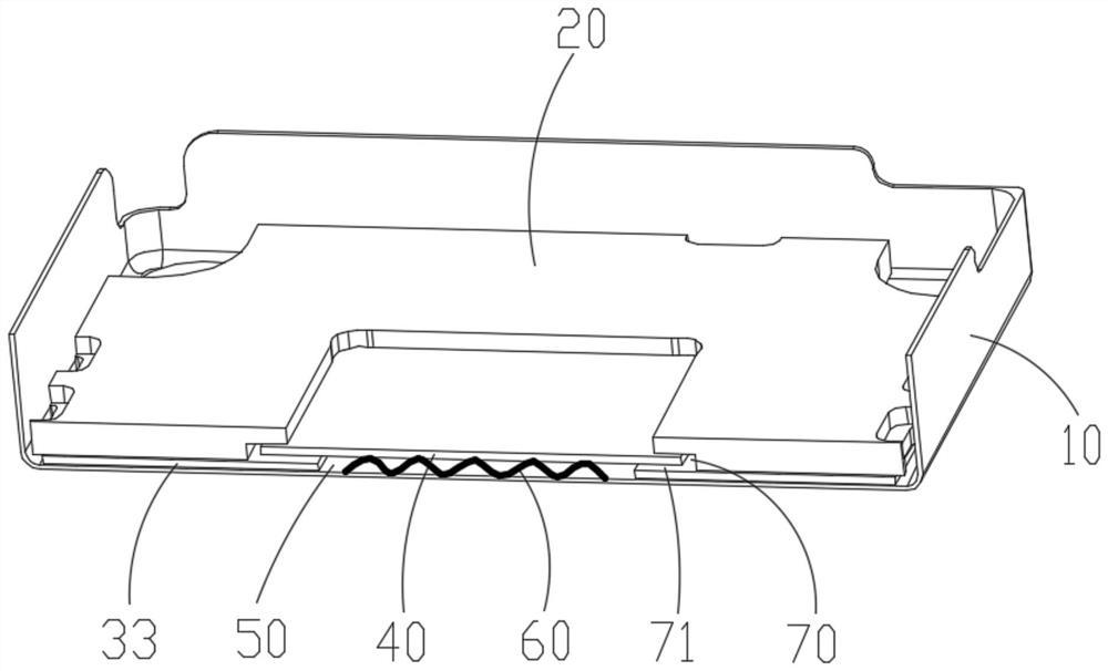
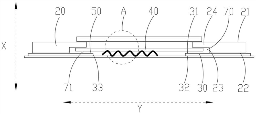
[0056] figure 1 A schematic structural diagram of an image sensor assembly provided in an embodiment of the present application, figure 2 for figure 1 Side view of the image sensor assembly shown.

[0057] like figure 1 and figure 2 As shown, this embodiment provides an image sensor assembly, including:

[0058] housing 10;

[0059] The base plate 20 is located in the housing 10 and includes an upper surface 21 and a lower surface 22 opposite to each other and a side surface 23 connected between the upper surface 21 and the lower surface 22, and the side surface 23 close to the upper surface 21 is convex on the side There is an installation part 24;

[0060] The flexible board 30 is located in the housing 10 and includes a first surface 31 and a second surface 32 opposite to each other, one end of the first surface 31 is connected with the lower surface 22 of the substrate 20 and the second surface 32 is connected with the housing 10 , the flexible board 30 is also pr...

Embodiment 2

[0086] like figure 1 and figure 2 As shown, this embodiment provides an image sensor assembly, including:

[0087] housing 10;

[0088] The base plate 20 is located in the housing 10 and includes an upper surface 21 and a lower surface 22 opposite to each other and a side surface 23 connected between the upper surface 21 and the lower surface 22, and the side surface 23 close to the upper surface 21 is convex on the side There is an installation part 24;

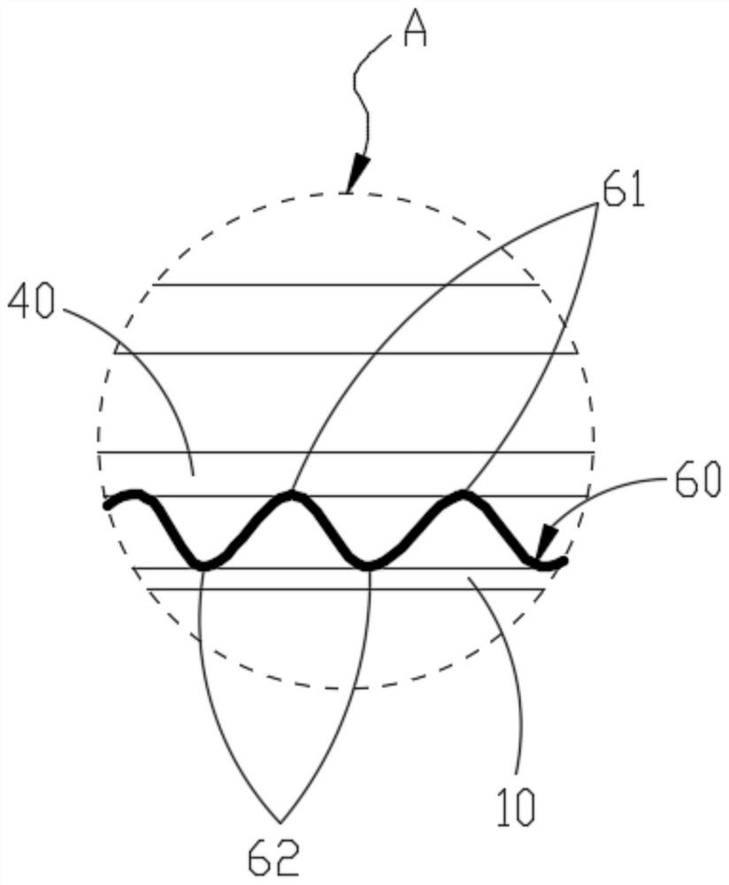
[0089] The flexible board 30 is located in the housing 10 and includes a first surface 31 and a second surface 32 opposite to each other, one end of the first surface 31 is connected with the lower surface 22 of the substrate 20 and the second surface 32 is connected with the housing 10 , the flexible board 30 is also provided with a through port 33;

[0090] The image sensor chip 40 is located in the casing 10 and is connected to one surface of the mounting portion 24 close to the lower surface 22 of the substrate 20 a...

Embodiment 3

[0113] like figure 1 and figure 2 As shown, this embodiment provides an image sensor assembly, including:

[0114] housing 10;

[0115] The base plate 20 is located in the housing 10 and includes an upper surface 21 and a lower surface 22 opposite to each other and a side surface 23 connected between the upper surface 21 and the lower surface 22, and the side surface 23 close to the upper surface 21 is convex on the side There is an installation part 24;

[0116] The flexible board 30 is located in the housing 10 and includes a first surface 31 and a second surface 32 opposite to each other, one end of the first surface 31 is connected with the lower surface 22 of the substrate 20 and the second surface 32 is connected with the housing 10 , the flexible board 30 is also provided with a through port 33;

[0117] The image sensor chip 40 is located in the casing 10 and is connected to one surface of the mounting portion 24 close to the lower surface 22 of the substrate 20 a...


PUM


Abstract

An image sensor assembly includes: a housing; the substrate is located in the shell and comprises an upper surface, a lower surface and a side surface, the upper surface and the lower surface are opposite, the side surface is connected between the upper surface and the lower surface, and one side, close to the upper surface, of the side surface is convexly provided with a mounting part; the soft plate is located in the shell and comprises a first surface and a second surface which are opposite to each other, one end of the first surface is connected with the lower surface, the second surface is connected with the shell, and a through opening is further formed in the soft plate; the image sensor chip is located in the shell, one end of the image sensor chip is connected to the surface, close to the lower surface, of the mounting part, the other end of the image sensor chip and the first surface are oppositely arranged in a spaced mode, and a closed cavity is defined by the image sensor chip, the soft board, the substrate and the shell; the elastic heat conduction piece is located in the cavity and has heat conductivity and elasticity, one end of the elastic heat conduction piece is connected with the image sensor chip, the other end of the elastic heat conduction piece penetrates through the through opening and then is connected with the shell, and the elastic heat conduction piece can deform after being extruded by the image sensor chip and the shell.

Description

technical field [0001] The present application relates to the technical field of image sensors, and in particular, to an image sensor assembly, a camera module and a mobile device. Background technique [0002] The advent of small mobile multipurpose devices, such as smartphones, tablets or tablet devices, has led to an increasing demand for high resolution, small form factor camera modules that can be integrated into the device. [0003] The camera module includes structures such as a camera module chip, a plurality of lenses, and a circuit board, and changes in temperature will cause thermal expansion and contraction of various components of the camera module, thereby causing the optical focus of the camera module to shift. Moreover, with the complexity of the integrated circuit of the camera module chip and the circuit board, the high temperature will also affect the function and service life of the electronic components of the camera module. [0004] In the Chinese inve...

Claims


Application Information

Patent Timeline
Patent Type & Authority Applications(China)
IPC IPC(8): H04N5/225G03B17/55
CPCG03B17/55H04N23/52H04N23/50
Inventor 杨银凯王慧
Owner NINGBO SUNNY OPOTECH CO LTD
Why Eureka
Try Eureka