Check patentability & draft patents in minutes with Patsnap Eureka AI!

Signal sampling circuit and semiconductor memory

A signal sampling and sampling circuit technology, applied in static memory, instruments, etc., can solve problems such as timing deviation and large timing deviation

Pending Publication Date: 2022-06-28
CHANGXIN MEMORY TECH INC
View PDF0 Cites 3 Cited by
  • Summary
  • Abstract
  • Description
  • Claims
  • Application Information

AI Technical Summary

Problems solved by technology

In this way, after the CA signal is sampled, because the instruction still needs to be decoded, the instruction path has more logic circuits for decoding than the address path, causing the instruction signal and address signal to have a relatively large gap when they reach the next-level functional module. Large timing deviation, which in turn leads to problems with the next-level functional modules due to timing deviation

Method used


Image

  • Signal sampling circuit and semiconductor memory
  • Signal sampling circuit and semiconductor memory
  • Signal sampling circuit and semiconductor memory

Examples


Embodiment Construction

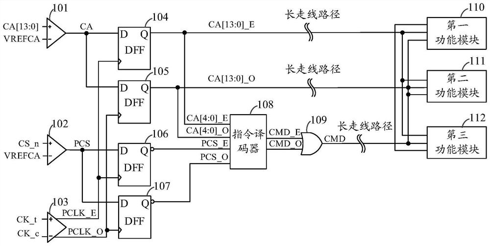
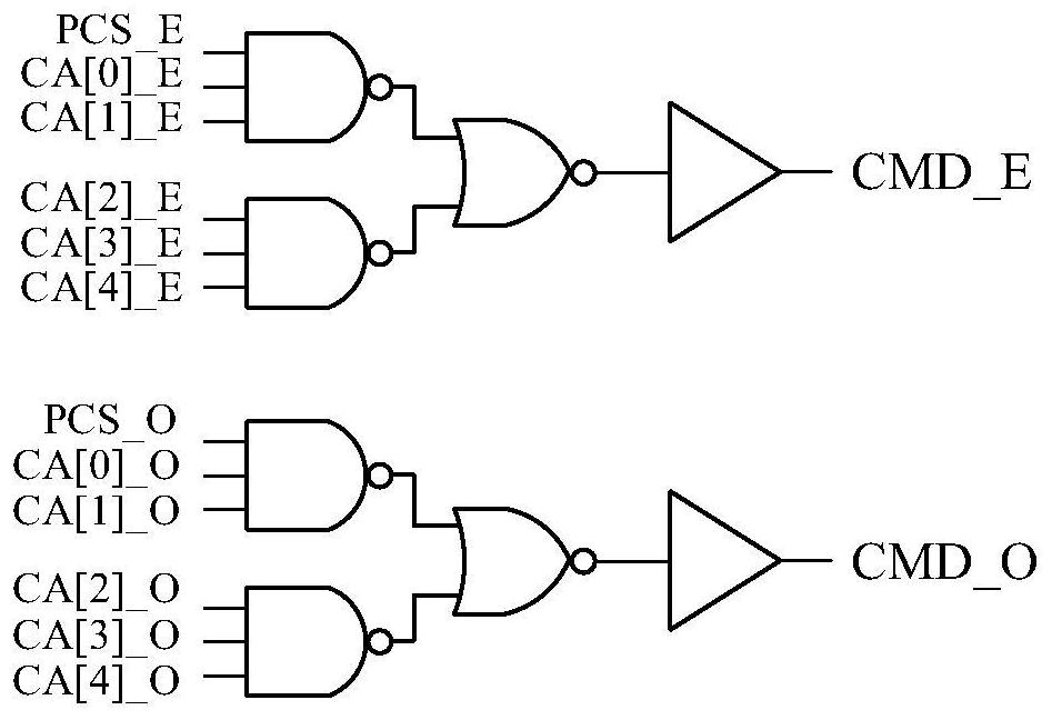
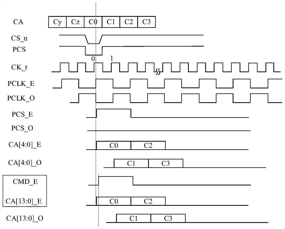
[0072] The technical solutions in the embodiments of the present disclosure will be clearly and completely described below with reference to the accompanying drawings in the embodiments of the present disclosure. It should be understood that the specific embodiments described herein are only used to explain the related application, but not to limit the application. In addition, it should be noted that, for the convenience of description, only the parts related to the relevant application are shown in the drawings.

[0073] Unless otherwise defined, all technical and scientific terms used herein have the same meaning as commonly understood by one of ordinary skill in the art to which this disclosure belongs. The terminology used herein is for the purpose of describing the embodiments of the present disclosure only and is not intended to limit the present disclosure.

[0074] In the following description, reference is made to "some embodiments" which describe a subset of all po...


PUM


Abstract

The embodiment of the invention provides a signal sampling circuit and a semiconductor memory, and the signal sampling circuit comprises an input sampling circuit which is used for carrying out the sampling processing of a first chip selection signal and a first command address signal according to a first clock signal, and obtaining a second chip selection signal and a second command address signal, the second command address signal comprises an initial command signal; the logical operation circuit is used for performing logical operation on the first clock signal and the second chip selection signal to obtain a chip selection clock signal; the instruction decoding circuit is used for decoding and sampling the initial instruction signal according to the chip selection clock signal and the second chip selection signal to obtain a target instruction signal; and the merging output circuit is used for carrying out sampling and output merging processing on the second command address signal according to the chip selection clock signal to obtain a target address signal. Therefore, time sequence alignment between the target address signal and the target instruction signal can be realized.

Description

technical field [0001] The present disclosure relates to the technical field of integrated circuits, and in particular, to a signal sampling circuit and a semiconductor memory. Background technique [0002] With the continuous development of semiconductor technology, people have put forward higher and higher requirements for the transmission speed of data when manufacturing and using equipment such as computers. In order to obtain a faster data transmission speed, a series of devices such as memories that can transmit data at a double rate (Double Data Rate, DDR) have emerged. [0003] In a dynamic random access memory (Dynamic Random Access Memory, DRAM), a command address (Command / Address, CMD / ADD or CA for short) signal can be sampled as an address and can be sampled and decoded as an instruction. In this way, after the CA signal is sampled, since the instruction still needs to be decoded, the instruction path has more logic circuits for decoding than the address path, c...

Claims


Application Information

Patent Timeline
IPC IPC(8): G11C29/12G11C29/14
CPCG11C29/12015G11C29/14G11C11/4076G11C8/06G11C11/4093G11C7/109G11C8/12G11C7/1093G11C7/22G11C7/222G11C7/225
Inventor 黄泽群
Owner CHANGXIN MEMORY TECH INC
Features
  • R&D
  • Intellectual Property
  • Life Sciences
  • Materials
  • Tech Scout
  • Unparalleled Data Quality
  • Higher Quality Content
  • 60% Fewer Hallucinations
Learn More