Supercharge Your Innovation With Domain-Expert AI Agents!

Photomask and method for inspecting photomask

A photomask and mask technology, which is applied to the original parts, optics, and optomechanical equipment used for photomechanical processing, and can solve the problems of misrecognized mask defect aggravation, degradation of total productivity, and heavy manpower burden.

Pending Publication Date: 2022-07-01
TAIWAN SEMICON MFG CO LTD
View PDF0 Cites 0 Cited by
  • Summary
  • Abstract
  • Description
  • Claims
  • Application Information

AI Technical Summary

Problems solved by technology

The problem of misidentifying mask defects is exacerbated by the requirement of complex design rules
Reviewing inspection results and manually filtering defects to be fixed and misidentifying defects will cause heavy manpower burden and degrade overall productivity

Method used

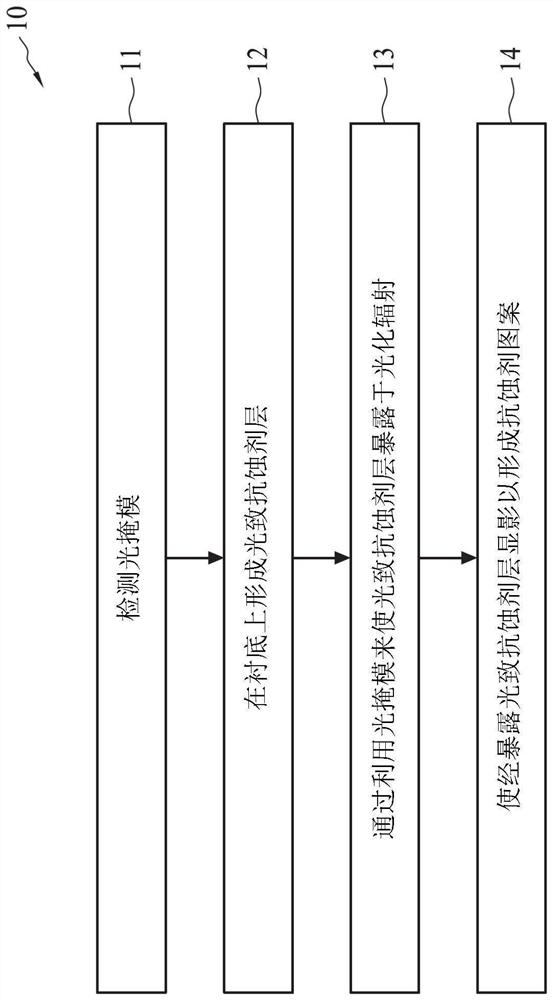
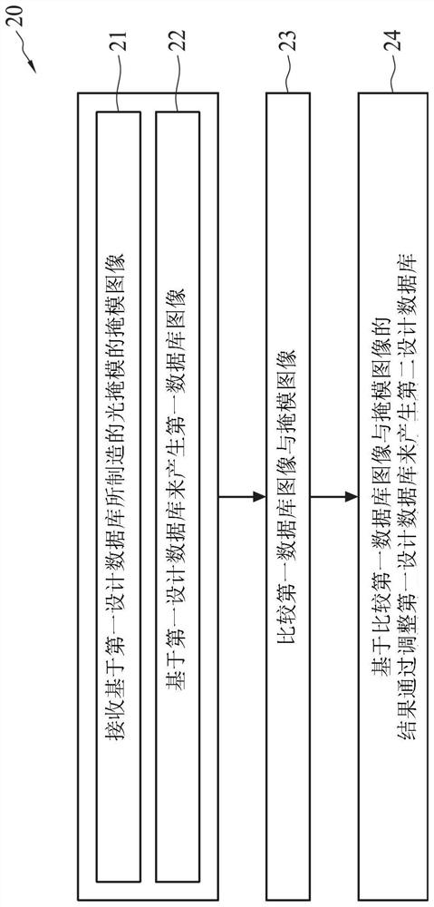
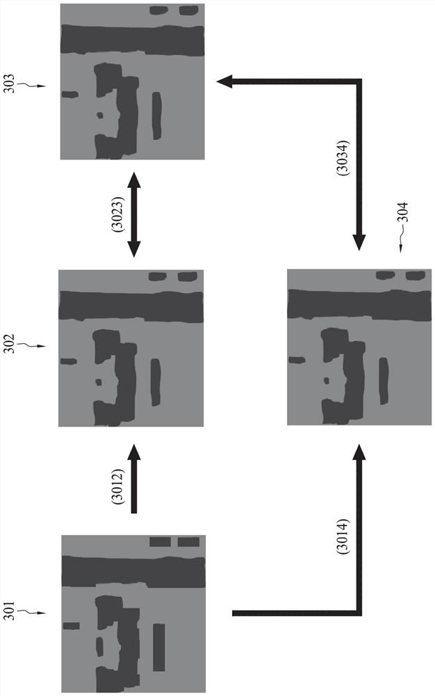

Image

  • Photomask and method for inspecting photomask
  • Photomask and method for inspecting photomask
  • Photomask and method for inspecting photomask

Examples


Embodiment Construction

[0026] The following disclosure provides many different embodiments or examples for implementing different features of the provided subject matter. Specific examples of components and arrangements are described below to simplify the present disclosure. Of course, these are only examples and are not intended to be limiting. For example, in the following description, forming a first feature over or on a second feature may include embodiments of the first feature and the second feature in which direct contact is formed, and may also include additional features in which Embodiments may be formed between the first feature and the second feature such that the first feature and the second feature may not be in direct contact. Additionally, the present disclosure may repeat reference numerals and / or letters in various instances. This repetition is for simplicity and clarity and does not in itself indicate the relationship between the various embodiments and / or configurations discuss...


PUM


Abstract

The embodiment of the invention relates to a photomask and a method for inspecting the photomask. Embodiments of the invention provide a photomask comprising: a plurality of pattern regions, each of the pattern regions being defined by a respective boundary, a first pattern region comprising a first mask feature; and a training region adjacent a boundary of the pattern region, the training region including a first training feature, where the first training feature is comparable to the first mask feature.

Description

technical field [0001] Embodiments of the present invention relate to photomasks and methods of inspecting photomasks. Background technique [0002] An integrated circuit (IC) is formed by first generating an integrated circuit design on a computer that describes the physical layout of the integrated circuit. Next, a photomask is formed from the IC design. Photomasks are used during IC fabrication to pattern semiconductor substrates to form on-chip structures corresponding to the IC design. In the production of semiconductors, lithography is performed using ultraviolet light sources or other radiation beams such as ion beams, X-rays, extreme ultraviolet (EUV) and deep ultraviolet (DUV). Photomasks are typically inspected for mask defects before being used to replicate mask images on semiconductor substrates used in products. If mask defects are detected, such defects can be repaired so that the mask defects do not replicate on the semiconductor substrate. [0003] Howeve...

Claims


Application Information

Patent Timeline
Patent Type & Authority Applications(China)
IPC IPC(8): G03F1/38G03F1/44G06F16/583
CPCG03F1/38G03F1/44G06F16/583G03F1/84G03F7/7065G03F1/76G03F1/70
Inventor 赖建宏张浩铭王宣文杨敬亭陈政光黄健朝
Owner TAIWAN SEMICON MFG CO LTD
Features
  • R&D
  • Intellectual Property
  • Life Sciences
  • Materials
  • Tech Scout
  • Unparalleled Data Quality
  • Higher Quality Content
  • 60% Fewer Hallucinations
Learn More