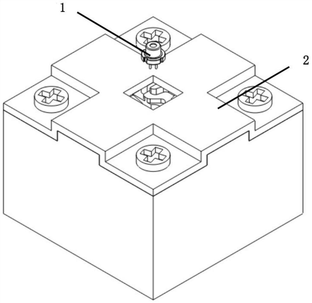
Short lead semiconductor laser and test fixture and test method thereof
A technology for testing fixtures and lasers, which is applied in the direction of semiconductor lasers, lasers, and laser components, etc., and can solve problems such as difficult lead wire fixing, inability to check electrical parameters, and single internal interconnection structure
- Summary
- Abstract
- Description
- Claims
- Application Information
AI Technical Summary
Problems solved by technology
Method used
Image
Examples
Embodiment 1
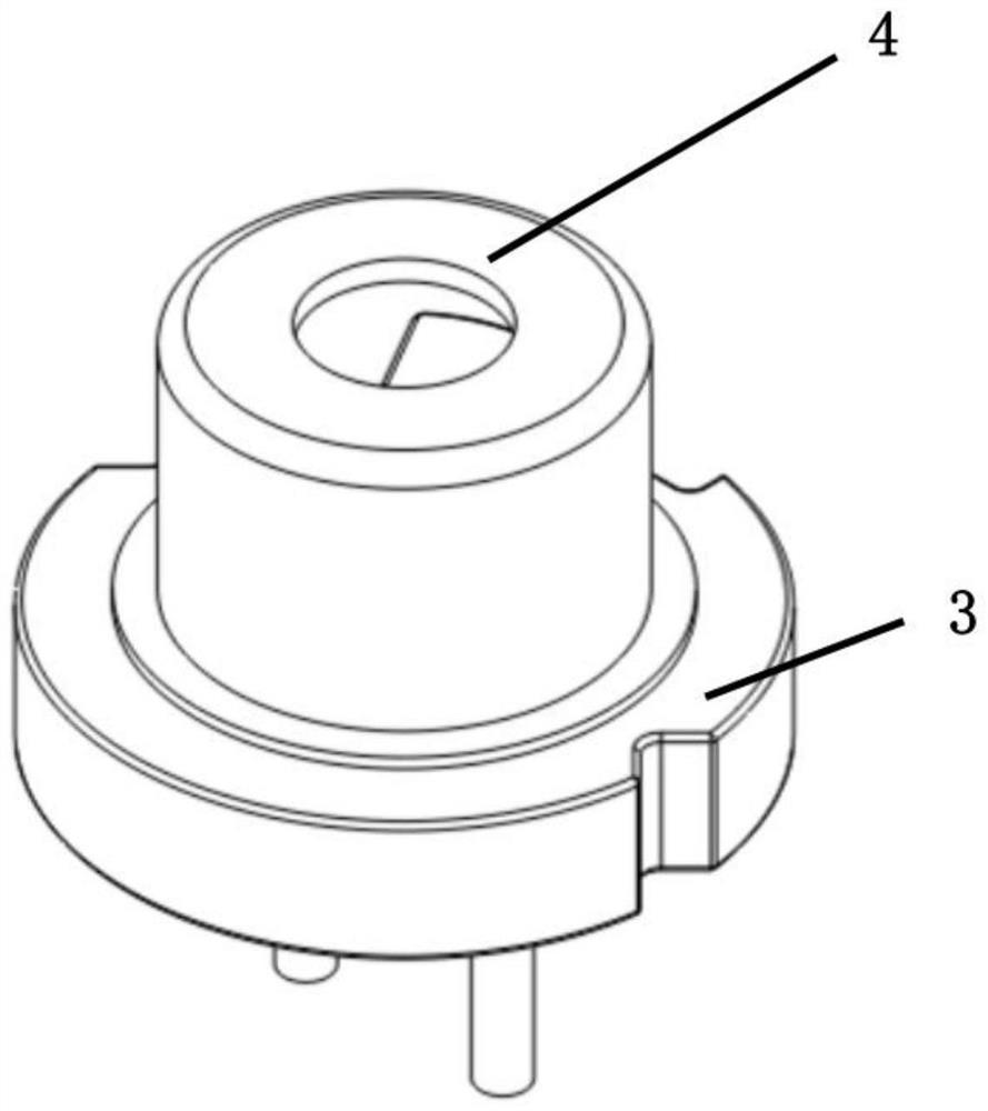
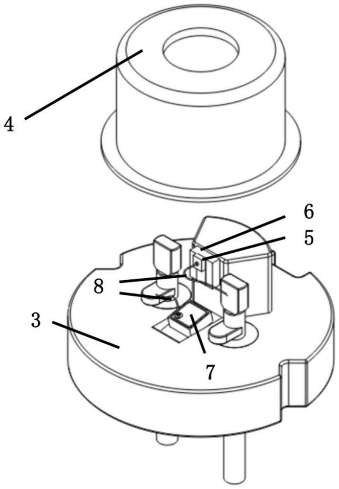
[0059] A short lead semiconductor laser such as Figure 2-1 , Figure 2-2 As shown, it includes a tube base 3, a tube cap 4, a laser chip 5, a transition heat sink 6, a PD chip 7, and a gold wire 8; the laser chip is sintered on the transition heat sink, and the transition heat sink and the PD chip are bonded to the tube base. .
[0060] The light-emitting surface of the laser chip faces outward, and the backlight surface faces the PD chip. The laser chip and the PD chip are each connected through gold wires.
[0061] The tube cap is welded on the tube base, and there is an opening outside the light-emitting surface of the laser chip.
[0062] The socket includes a base plate 9, a pipe tongue 10, and a lead wire 11; a positioning gap 13 is provided on the side of the base plate, which is used for packaging and direction positioning during use; the pipe tongue is set on the surface of the base plate, and the pipe tongue is a cylinder with a fan-shaped cross-section. A die bo...
Embodiment 2
[0065] A short-lead semiconductor laser, the structure of which is as described in Embodiment 1, the difference is that the number of leads is three, of which two leads (ie, left and right). Figure 3-1 An insulating glass 12 is provided between the exposed leads) and the substrate, such as Figure 3-2 As shown, the insulating glass isolates the leads from the substrate, and a middle lead is directly sintered on the lower surface of the substrate and conducts with the substrate and the tongue.
[0066] The second welding platform perpendicular to the lead is located above the insulating glass, used for PD chip bonding, and the second welding platform parallel to the lead is located above the second welding platform perpendicular to the lead, at the top end of the lead, used for laser chips and transition heat Solder wire. The entire tube base structure is left and right symmetrical.
Embodiment 3
[0068] A short lead semiconductor laser, the structure of which is as described in Embodiment 1, and the short lead semiconductor laser comprises one of the following schemes:
[0069] ⅰ. The positive electrode or negative electrode of the laser chip is facing the transition heat sink;
[0070] 2. Use conductive materials (such as copper, silicon, etc.) or non-conductive materials (such as aluminum nitride, etc.) for the transition heat sink; sintering the laser chip with the solder on the upper surface, and sintering the tongue with the solder on the lower surface to form a good ohmic contact;
[0071] iii. The PD chip uses P-type substrate or N-type substrate;
[0072] iv. The upper surface of the PD chip is single electrode or double electrode.
[0073] The gold wire forms interconnection between the laser chip, the PD chip, the transition heat sink, the tube tongue, and the lead wire, and according to design requirements, a variety of different lead wire definitions can b...
PUM
 Abstract
Description
Claims
Application Information


